I. Introduction
1.1 Background and Purpose of the Study
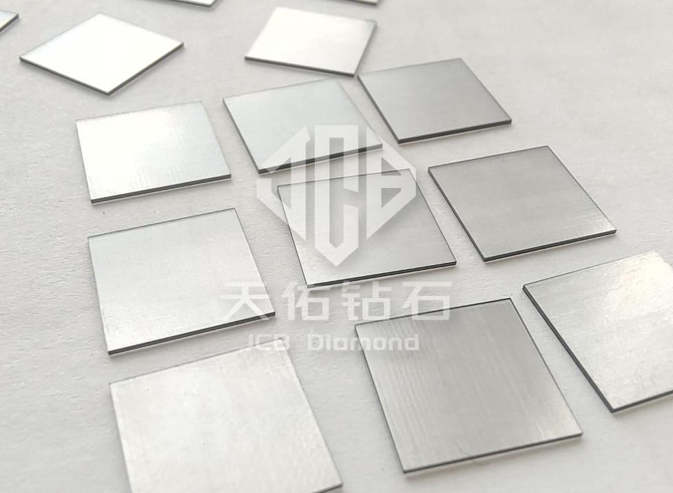
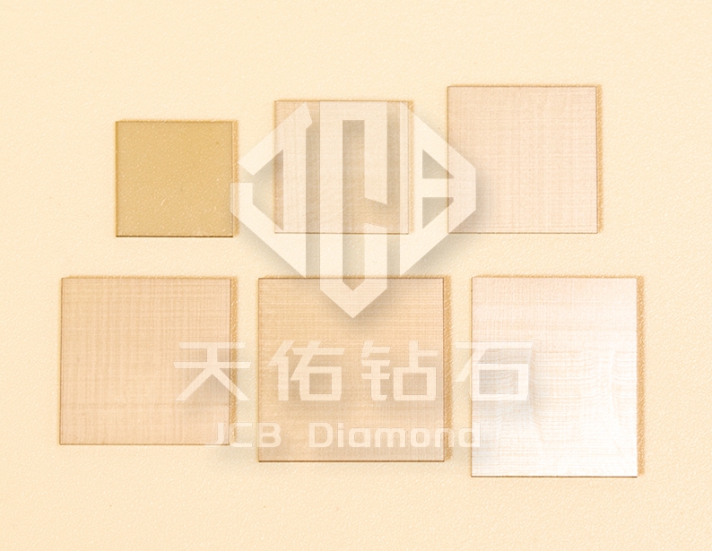
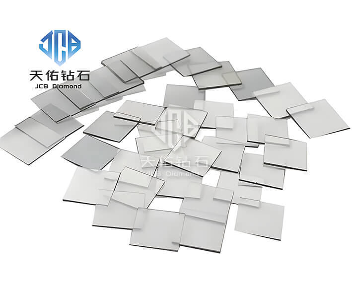
Chemical Vapour Deposition (CVD) seed, as a key element in the field of modern materials science, plays an indispensable role as a cornerstone in many industries such as semiconductors, superhard materials, optics, etc. With the rapid development of science and technology, the demand for high-performance materials is exploding in various industries. With the rapid development of science and technology, the demand for high-performance materials in various industries has exploded, and CVD crystals have become the core force to satisfy these demands by virtue of their unique advantages, such as precise control of crystal structure, high purity, and the ability to achieve the deposition of complex shapes, etc. In the field of semiconductors, CVD crystals have become the core force to satisfy the demand for high-performance materials.
In the semiconductor field, in order to cope with the trend of miniaturisation, high performance and high integration of electronic products, there is an urgent demand for large-size and high-quality single crystal materials, and CVD seeds used in the preparation of semiconductor single crystals can effectively improve key performance indicators such as electron mobility and breakdown electric field, helping chip performance leap, and providing solid guarantees for the hardware foundations of cutting-edge technologies such as 5G communications, artificial intelligence and quantum computing. Solid guarantee. In the field of superhard materials, artificial diamond and other superhard materials are widely used in industrial processing, resource extraction, etc. CVD seed technology can break through the limitations of traditional preparation methods, achieve the synthesis of larger size and higher quality superhard materials, significantly improve the hardness and wear resistance of materials, reduce production costs, and promote the development of machinery manufacturing, geological exploration and other industries. In the field of optics, optical crystals prepared by CVD grades have shown excellent optical properties in laser technology and optical instruments, such as high transmittance and low absorption coefficients, which have strongly promoted the innovation of optical technology.
However, CVD seed technology still faces many challenges. The complexity of the preparation process, harsh equipment requirements, and the need for extremely high parameter control accuracy have resulted in high preparation costs and difficulty in improving yield rates, making it difficult to meet the demands of large-scale industrial production. Different application scenarios have different performance requirements for CVD chips, such as the semiconductor field focusing on electrical performance and the optical field focusing on optical performance, so how to accurately regulate the microstructure and composition distribution of the chips to meet diversified needs is a difficult problem that needs to be solved urgently. Moreover, the global market competition is fierce and the technological upgrading is accelerating. Although China has made some progress in the CVD seed industry, there is still a gap between the high-end products and core technologies and the international advanced level, and we are facing the double pressure of technological embargo and market extrusion.
This study aims to comprehensively analyse the development status quo of CVD chips, deeply explore the technical bottlenecks, and systematically explore the future development direction and innovation strategy, so as to provide decision-making basis and intellectual support for the technological breakthrough and industrial upgrading of China's CVD chips, and help China stand out from the competition in the global new materials industry, and seize the scientific and technological vantage point.
1.2 Research Methods and Scope
This study makes comprehensive use of a variety of research methods to explore the field of CVD crystal seed in an all-round and deep level. By extensively reviewing domestic and international academic literature, patent information and industry reports, we systematically sort out the basic theories, technological evolution, patent layout and market dynamics of CVD varieties, so as to build up a solid research knowledge framework and accurately grasp the frontiers of the discipline and industrial trends; we conduct in-depth research on enterprises and research institutes, collect typical cases, and analyse the successful experiences and practical dilemmas, so as to inject realistic vitality into the theoretical research; we use data analysis to analyze the CVD varieties, and we also use the data analysis method to analyze the CVD varieties. Using data analysis tools, we conduct statistical analyses on quantitative indicators such as market size, growth trend, and competition pattern of CVD chips to gain a comprehensive insight into the development of the industry.
The scope of the research covers the whole life cycle of CVD seeds, starting from the preparation technology, analyzing in detail the principle, process, advantages and disadvantages of mainstream preparation methods, and exploring the path of equipment selection and process optimization; analyzing in depth the physical, chemical, electrical and optical properties of the seeds, explaining the intrinsic correlation between the properties and microstructures and compositions, and constructing a theoretical model for the control of properties; and comprehensively expanding to multiple application fields, such as semiconductors, superhard materials, optics, energy, etc., to study the development of the industry, We will comprehensively expand to semiconductor, superhard materials, optics, energy and other diversified application fields, and study the suitability, application effect and innovation breakthrough point of crystalline species in each field; we will focus on the global and Chinese markets, and interpret the industrial policies, competitive situation and development opportunities, so as to clarify the strategic direction for industrial participants.
Overview of CVD Technology
2.1 Classification and Characteristics of CVD Technology
CVD technology can be subdivided into various types according to the difference of energy supply mode and reaction conditions. Thermal chemical vapour deposition (Thermal CVD) is the most basic and widely used type, in which the gaseous reactants are decomposed and reacted by heating the reaction chamber. For example, in the preparation of silicon nitride (Si₃N₄) thin film, the silicon source gas and ammonia are reacted at a high temperature (usually 700-1200°C), which can obtain a high-quality and dense thin film, and the advantages of this technique are simple equipment and mature process, and the disadvantages are that the deposition gas is not as strong as the other gases. The advantages are simple equipment, mature process, the disadvantage is that the deposition temperature is high, easy to cause thermal damage to the substrate, not applicable to heat-sensitive materials.
Plasma-enhanced chemical vapour deposition (PECVD) can be carried out at lower temperatures (200 - 400°C) by means of plasma-excited gaseous reactants, which reduces the activation energy required for the reaction. In the preparation of hydrogenated amorphous silicon (a-Si:H) films for amorphous silicon solar cells, PECVD avoids damage to the cell structure at high temperatures, improves productivity, and provides the flexibility to adjust plasma parameters to control film properties, but the introduction of plasma may result in a small number of defects in the film, such as pinholes and uneven density.
Laser chemical vapour deposition (LCVD) uses a high-energy laser beam focused on a reaction region on the substrate surface to instantly raise the local temperature and initiate a gas-phase reaction. This method enables high-precision micro-area deposition for the preparation of materials with tiny sizes and special structures, such as nanoscale functional coatings in microsensors, with relatively low deposition rates, high equipment costs, and demanding operating techniques.
Different types of CVD technologies have their own characteristics in terms of temperature, pressure, deposition rate, film quality and other key indicators. Thermal CVD has high deposition temperature, wide pressure range, medium deposition rate, high film quality but high risk of thermal damage to the substrate; PECVD has low temperature, moderate pressure, fast deposition rate, good film quality but with hidden defects; LCVD can achieve local high temperature, low pressure, slow deposition rate, but can achieve high-precision micro and nanostructures deposition, and the quality of the film depends on the precision of laser parameter regulation.
CVD Grades Application Fields

3.1 Application in Semiconductor Industry
3.1.1 Advantages as a substrate material
In the booming wave of semiconductor industry, CVD seeds as a substrate material is like a shining pearl, emitting a unique light. Take silicon-based semiconductors as an example, the monocrystalline silicon substrate prepared by CVD varieties has excellent crystal integrity, the lattice defect density is greatly reduced compared with the traditional process, which can effectively reduce the centre of electron scattering, resulting in a significant increase in the electron mobility, and providing a solid foundation for high-speed electronic devices.
In the field of compound semiconductors, such as gallium nitride (GaN) crystal species used in the preparation of substrates, its precisely adjustable crystal orientation and uniformity, so that the semiconductor devices based on its growth in the light-emitting efficiency, power density and other key performance to achieve a quantum leap. Compared with sapphire and other traditional substrates, GaN seed substrate can significantly reduce the dislocation density, reduce internal stress, improve the quality of the epitaxial layer for high-performance LEDs, microwave power devices, such as large-scale industrialisation to clear the obstacles, and strongly promote semiconductor technology towards higher performance, lower power consumption, smaller size of the direction of progress.
3.1.2 Practical Application Cases and Achievements
TSMC, as a global leader in semiconductor manufacturing, widely applies CVD seed technology in its advanced process chip production line. By adopting customised CVD seeds and precisely controlling the growth of silicon epitaxial layers, TSMC has successfully manufactured high-performance chips at 7nm and below. In the manufacturing of 5G communication chips, these chips have demonstrated excellent high-frequency performance, with a 30% increase in signal transmission rate and a 20% reduction in power consumption, which meets the urgent demand for high-performance chips in 5G base stations, smartphones, etc., and solidifies TSMC's dominant position in the field of global high-end chip manufacturing, as well as injecting strong impetus into the development of the global 5G industry.
3.2 Application in the field of superhard materials
3.2.1 Preparation of superhard cutting tools and abrasives
In the field of superhard materials, CVD seed technology has become a core tool for the preparation of high-performance tools and abrasives. Take the cutting tool prepared by synthetic diamond crystal seed as an example, its hardness is as high as 100 - 150GPa, far more than the traditional cemented carbide cutting tools. In precision machining, such as aerospace engine blade processing, diamond crystal seed coated tools can achieve high precision cutting with very small cutting force, surface roughness up to Ra0.05 - 0.1μm, significantly extend tool life, reduce processing procedures, improve productivity by about 40%, effectively reduce production costs, and provide a solid guarantee for high-end equipment manufacturing.
3.2.2 Application in geological exploration
Geological exploration work is faced with a complex and changing geological environment, CVD crystal seed preparation of superhard materials in this show their skills. Drill bits made of superhard materials grown from CVD crystals, such as polycrystalline diamond composite (PDC) drill bits, can easily cope with hard rock formations by virtue of their ultra-high hardness, abrasion resistance and good impact toughness. In deep oil and gas exploration, PDC drill bits can increase the drilling speed by about 50% and extend the service life by 2-3 times compared with traditional tooth wheel drill bits, which can significantly reduce the drilling cost, improve the exploration efficiency, provide the key support for the development of global energy resources, and help mankind to move towards the exploration of the deep part of the earth.
3.3 Optical Applications
3.3.1 Optical Window and Lens Manufacturing
In the field of optics, the optical components made of CVD crystal species are like the ‘eyes’ of precision optical instruments, guaranteeing excellent optical performance. Take the optical window prepared by sapphire crystal species as an example, it has the characteristics of high hardness, high transmittance, wear resistance, etc. In aerospace optical remote sensing equipment, it can work stably under extreme temperature, pressure and complex radiation environment, and the transmittance rate can reach 80% - 90% in visible to infrared wavelengths, which ensures a clear imaging of the optical system, and provides accurate data support for the satellite observation of the earth and space exploration.
In terms of lens manufacturing, fluoride crystals grown by CVD can be used to manufacture ultraviolet lenses, which can effectively correct chromatic aberration and achieve high-precision focusing to meet the stringent requirements for high resolution and high imaging quality in photolithography, optical inspection and other high-end optical applications, and promote optical precision manufacturing to move forward to a higher precision and a wider wavelength band.
3.3.2 Foundation of Laser Crystal Growth
As the bright light of modern technology, laser technology, CVD crystal seeds play an indispensable role. Yttrium-aluminium-garnet (YAG) crystals, as the basis for growing laser crystals, can be precisely controlled in terms of doping concentration and uniformity through the precise CVD process. In high-power solid-state lasers, neodymium (Nd)-doped YAG crystal growth of laser crystals can achieve efficient light pumping absorption and energy conversion, the output power can reach several kilowatts or even higher, and is widely used in laser cutting, laser welding, laser marking and other industrial processing areas, significantly improving processing efficiency and quality, and empowering the transformation and upgrading of manufacturing industry.
