I. Industry Overview
1.1 Definition and Characteristics
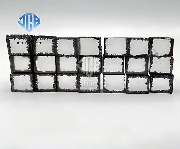
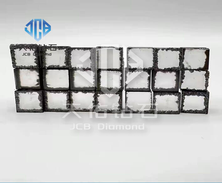
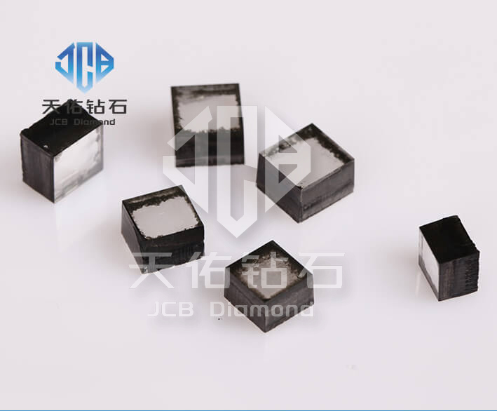
CVD (Chemical Vapor Deposition) single crystal diamond refers to single crystal diamond material prepared by chemical vapor deposition technology. It has the same crystal structure and chemical composition as natural diamond and has many excellent properties.
In terms of hardness, its Mohs hardness is as high as 10, which is the hardest substance known in nature. This enables it to accurately achieve mirror processing in the field of ultra-precision machining, such as machining ultra-precision mirror parts such as reflectors of nuclear reactors and precision optical instruments, computer hard disks, etc., to ensure extremely high dimensional accuracy and surface roughness as low as nanometer level.
In terms of thermal conductivity, the thermal conductivity of CVD single crystal diamond at room temperature can reach more than 2000W/(m·K), which is far higher than traditional heat dissipation materials such as copper and silver. It can quickly dissipate heat and is an ideal thermal management material. It is widely used in laser cooling systems, electronic chip cooling and other scenarios, which can effectively reduce operating temperature and improve equipment stability and life.
In terms of chemical stability, it has high chemical inertness, acid and alkali corrosion resistance, can maintain stable performance in harsh chemical environments, and is suitable for special fields such as chemical industry and biomedicine. The optical performance is even more outstanding, from 225nm in ultraviolet to 25μm in infrared (except for wavelengths of 1.8μm - 2.5μm), and to the microwave range, it has excellent transmittance. It is an excellent material for making modern infrared optical windows, optical lenses, prisms, etc., and plays a key role in aerospace, national defense, optical instruments and other fields.
1.2 Development History
The development of CVD technology to prepare single crystal diamond has a long history. In the early days, scientists were inspired by the formation process of natural diamonds and explored simulating their growth conditions in laboratory environments. In the mid-20th century, with the advancement of materials science and chemical engineering technology, CVD technology took shape and began to try to use a mixture of carbon-containing gas and hydrogen to decompose and deposit carbon atoms in a high temperature and low pressure environment. However, at this time, the crystal quality was poor and the growth rate was extremely low. Only tiny diamond particles with many defects could be prepared, which were mainly used for basic scientific research exploration.
In the 1980s and 1990s, with the introduction of microwave plasma technology into the CVD process, the emergence of microwave plasma chemical vapor deposition (MPCVD) brought a breakthrough in the growth of single crystal diamond. This method can produce highly active plasma, which allows carbon atoms to be deposited more efficiently and arranged in an orderly manner, significantly improves the crystal growth rate, gradually increases the size, and greatly improves the purity and quality. It has begun to be involved in industrial applications such as cutting tools and heat sinks, but the cost is still high and the technology is only in the hands of a few scientific research institutions and enterprises.
Entering the 21st century, global scientific research forces have continued to increase investment, equipment has been continuously improved and optimized, and process parameters have been finely controlled to achieve precise control of the crystal growth process. Not only can large-sized, high-quality single crystal diamonds be prepared, but also achievements have been made in doping modification, giving materials new electrical and optical properties, and expanding to cutting-edge high-tech fields such as semiconductors, quantum technology, and optoelectronic devices. The scale of the industry has also gradually expanded, from laboratories to industrial mass production. Many companies have made layouts to promote CVD single crystal diamonds to a broader application world.
2. Preparation process research
2.1 Main preparation methods
2.1.1 Microwave plasma CVD method (MPCVD)
Microwave plasma CVD method is one of the mainstream technologies for preparing high-quality CVD single crystal diamond. Its principle is to use a microwave generator to generate microwaves of a specific frequency (usually 2.45GHz), which are introduced into the reaction chamber to excite the carbon-containing gas (such as methane) and hydrogen mixed gas in the chamber under the action of the electromagnetic field to form a highly active plasma. In this plasma environment, gas molecules are highly ionized and dissociated, producing a large number of active groups, such as carbon atoms, hydrogen atoms and various carbon-hydrogen-containing active groups. These active species are adsorbed, diffused, and reacted on the substrate surface, and gradually deposited and crystallized to grow diamonds.
The Ningbo Institute of Materials Technology and Engineering, Chinese Academy of Sciences, uses MPCVD technology to achieve precise control of plasma density and distribution by optimizing microwave transmission mode and improving reaction chamber design. During the preparation process, they maintained the pressure of the reaction chamber at 20-30mbar and precisely controlled the microwave power at 1.5-2.5kW. The quality of the grown single crystal diamond crystals was significantly improved, the dislocation density was reduced by about 30% compared with the traditional process, and the optical transmittance could reach more than 70% in the 2-10μm band. It was successfully applied to high-end optical fields such as high-power laser windows, fully demonstrating the advantages of the MPCVD method in preparing high-quality single crystal diamond.
2.1.2 Hot Wire CVD Method (HFCVD)
The working principle of the hot wire CVD method is to use the metal wire (usually tungsten wire or tantalum wire) to heat it to a high temperature of 2000℃-2500℃, so that the introduced reaction gas (mainly a mixture of methane and hydrogen) undergoes a catalytic decomposition reaction on the surface of the hot wire. The high temperature generated by the hot wire causes hydrogen molecules to dissociate into hydrogen atoms, and methane to decompose into carbon-containing active groups. These active particles reach the substrate surface under the action of thermal convection and diffusion, and then deposit to form a diamond film.
SP3 Crystallame in the United States uses HFCVD technology for large-scale production. With its simple equipment and low cost, it has greatly reduced the preparation cost of diamond films. Compared with MPCVD equipment, the cost of HFCVD equipment can be reduced by about 40% - 50%, and it is easy to operate and maintain, and the technical requirements for operators are relatively low, which makes this technology have significant industrialization potential in industrial application fields such as tool coatings and heat sink materials. The market share is gradually expanding, especially in the low-end market.
2.1.3 Other methods
The DC plasma CVD method is to apply a DC voltage between the two poles of the reaction chamber to ionize the gas to form a plasma, accelerate the decomposition and deposition of carbon-containing gas to form diamond. The device structure of this method is relatively simple and the cost is low, but the plasma stability is poor, which easily leads to poor uniformity of diamond growth. It is often used in fields such as wear-resistant coatings that do not require high crystal quality.
The combustion flame CVD method uses the high-temperature flame zone generated by the combustion of mixed gases such as acetylene and oxygen as the reaction site. The high temperature in the flame causes the gas to decompose, and the generated activated carbon species are deposited on the substrate to grow diamonds. This method has a fast growth rate, but due to the complexity of the combustion process, it is difficult to accurately control the reaction parameters, and the quality of the prepared diamond fluctuates greatly. It is often used to prepare polycrystalline diamond films and applied to rough processing scenarios such as cutting tools. Compared with MPCVD and HFCVD, DC plasma CVD and combustion flame CVD differ in process complexity, crystal quality control, and application scenario targeting. They each play a role in specific segments and jointly enrich the preparation technology system of CVD single crystal diamond.
2.2 Process optimization research
2.2.1 Substrate selection and processing
As the basis for the growth of single crystal diamond, the substrate plays a key role in the quality of the crystal. Taking homoepitaxial growth as an example, a diamond substrate is used. Due to its high lattice matching with the growth layer, it can effectively reduce the dislocation density and facilitate the growth of high-quality single crystals. Studies have shown that when growing on a {100} oriented diamond substrate, the crystal growth rate can be stabilized at 2-3μm/h, and the crystal quality is excellent, and the dislocation density can be controlled below 10⁵ cm⁻². Although heterogeneous substrates such as silicon and sapphire are relatively low-cost and easy to obtain, they have a large lattice mismatch with diamond, which can easily induce stress and increase crystal defects. To improve this situation, when using a silicon substrate, a thin silicon carbide transition layer is first grown by chemical vapor deposition, which can effectively alleviate the lattice mismatch, increase the diamond nucleation density by about 20% - 30%, and promote single crystal growth.
Substrate pretreatment is also an important part of improving nucleation and growth quality. Mechanical grinding of the substrate to make its surface roughness reach the nanometer level can greatly increase the nucleation sites; combined with ultrasonic cleaning to remove surface impurities, it can create a clean environment for diamond growth and significantly improve the nucleation uniformity and growth stability.
2.2.2 Gas flow and ratio control
Gas flow and ratio are directly related to the diamond growth process. Experimental data show that when the methane to hydrogen flow ratio is adjusted from 1:100 to 1:50, the diamond growth rate can be increased by about 30% - 40%, but too high a methane ratio will lead to an increase in graphite phase inclusions, affecting the crystal quality. By precisely controlling the methane flow rate at 2-5sccm and the hydrogen flow rate at 100-200sccm, graphitization can be effectively inhibited while ensuring a certain growth rate, thereby improving the purity of the crystal and reducing internal defects, meeting the requirements of different applications for crystal quality, such as ensuring high transparency and low absorption loss in the preparation of optical-grade single-crystal diamond.
2.2.3 Temperature and pressure control
Temperature has a significant impact on the diamond crystallization process. In the MPCVD process, the temperature is usually controlled at 800℃-1000℃. If the temperature is too high, the atomic diffusion rate on the diamond surface is too fast, and secondary nucleation is easily formed, resulting in a rough crystal surface and more defects; if the temperature is too low, atomic migration is limited and the growth rate is slow. In terms of pressure, the reaction chamber pressure is generally maintained at 10-50mbar. Properly increasing the pressure can increase the probability of gas molecule collisions and promote carbon atom deposition, but too high pressure will make the plasma unstable and affect growth uniformity.
Today, advanced equipment is equipped with high-precision temperature sensors and pressure control systems, such as intelligent temperature control systems based on feedback control, which can control temperature fluctuations within ±5°C and pressure fluctuations within ±1mbar, ensuring that the parameters of each preparation process are highly consistent, greatly improving the stability and repeatability of product quality, and laying a solid foundation for the industrial mass production of CVD single crystal diamond.
3. Exploration of application fields
3.1 Electronic device field
3.1.1 Heat dissipation application
In the field of heat dissipation of electronic devices, CVD single crystal diamond plays a key role with its ultra-high thermal conductivity. Taking power semiconductor devices as an example, as semiconductor technology develops towards high power and high integration, the power density of chips has risen sharply, and heat dissipation has become a bottleneck restricting performance improvement. Traditional heat dissipation materials such as copper and aluminum usually have thermal conductivity of 200-400W/(m·K), which is difficult to meet the heat dissipation requirements of high-power chips.
The room temperature thermal conductivity of CVD single crystal diamond can reach more than 2000W/(m·K), which can quickly conduct the heat generated by the chip and effectively reduce the operating temperature of the chip. Experimental data show that under the same heat dissipation conditions, the junction temperature of power semiconductor devices using CVD single crystal diamond heat sinks can be reduced by 20-30℃ compared to copper heat sinks, which greatly improves the reliability and service life of the devices and reduces performance degradation and failures caused by overheating. It is widely used in electronic devices with strict heat dissipation requirements, such as 5G base station power amplifiers and new energy vehicle motor controllers.
3.1.2 Semiconductor substrate materials
As a semiconductor substrate material, CVD single crystal diamond has unique advantages. In terms of high-speed electron migration characteristics, its electron mobility can reach 4500cm²/(V·s) at room temperature, which is much higher than traditional semiconductor substrate materials such as silicon (1500cm²/(V·s)) and gallium arsenide (8500cm²/(V·s)). This enables electronic devices based on diamond substrates to achieve higher switching speeds and frequency responses, and is suitable for cutting-edge fields such as high-frequency and high-speed communications, such as RF front-end chips in 5G and 6G communication base stations.
In terms of low power consumption, diamond's high breakdown electric field (up to 10⁹ V/cm) can withstand higher voltages, reduce leakage, and reduce power consumption. However, CVD single-crystal diamond also faces challenges in its application as a semiconductor substrate. On the one hand, the cost remains high. The current process for preparing large-size, high-quality single-crystal diamond substrates is complex and the equipment is expensive, resulting in material costs far exceeding silicon and silicon carbide substrates, limiting large-scale commercial applications; on the other hand, it is not compatible with existing semiconductor processes. When integrated with silicon-based, compound semiconductors and other materials, there are problems such as lattice mismatch and thermal expansion coefficient differences. It is necessary to develop special processes and interface processing technologies to achieve good heterogeneous integration and promote the application of diamond substrates in the next generation of semiconductor industry.
3.2 Optical field
3.2.1 Optical window materials
In the field of optics, CVD single-crystal diamond is extremely valuable as an optical window material. In the infrared optical window application scenario, for some optical detection equipment in special environments, such as military infrared thermal imagers, infrared remote sensing windows of spacecraft, etc., the window material is required to have the characteristics of wide spectrum light transmittance, high hardness, wear resistance, and strong chemical stability.
CVD single crystal diamond has excellent transmittance from 225nm in ultraviolet to 25μm in infrared (except for wavelengths of 1.8μm - 2.5μm), and in the microwave range, with a theoretical transmittance of up to 71.6%, which can meet the needs of complex optical systems for wide-band light transmission. Its hardness is as high as Mohs 10, which can effectively resist the wear caused by harsh environments such as sand and dust, high-speed airflow impact, and ensure the long-term stable operation of the optical window. Compared with traditional infrared optical window materials such as germanium and zinc sulfide, it has significant advantages in durability and comprehensive optical performance.
3.2.2 Application of laser devices
CVD single crystal diamond also performs well in laser devices. In high-power laser resonant cavity applications, the high energy density laser generated by the laser when it is working is easy to damage the resonant cavity material, while single crystal diamond has a high laser damage threshold and can withstand extremely high light intensity, ensuring the stable operation of the resonant cavity and maintaining the stability and efficiency of the laser output.
As an optical gain medium, diamond has a high Raman gain coefficient. Based on the principle of stimulated Raman scattering, it can achieve flexible conversion and expansion of laser wavelengths. For example, under specific pumping conditions, the pump light wavelength can be converted to a new Stokes wavelength to meet the wavelength diversification requirements of different laser processing, laser medical treatment and other applications. At the same time, its excellent thermal conductivity helps to quickly dissipate the heat generated by the laser, effectively solve thermal management problems such as thermal lens effect, ensure the beam quality and performance of laser devices under high-power operation, and provide solid support for the development of advanced laser technology.