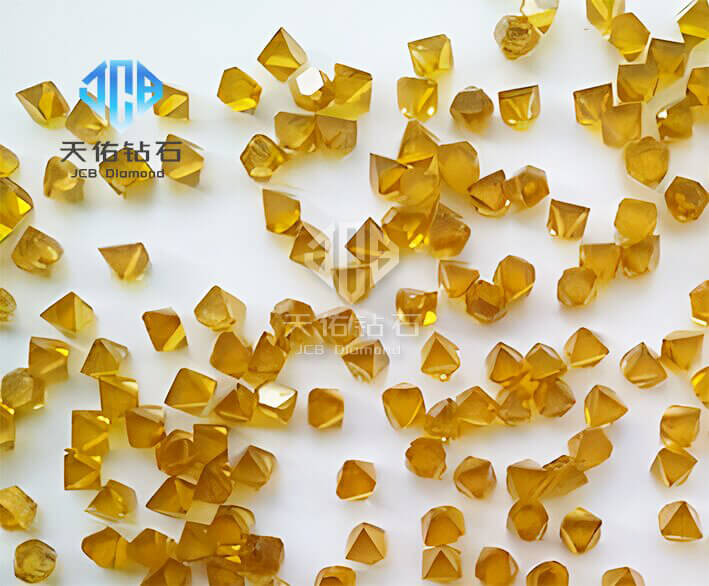
Microstructural Differences: Single-crystal diamond possesses a highly regular, nearly perfect crystal structure. At the atomic scale, carbon atoms are arranged in a tightly ordered, three-dimensional, periodic pattern, creating a seamless and coherent lattice. The entire crystal germinates from a single nucleus and grows steadily along a specific crystallographic direction, uninterrupted by grain boundaries. This results in an even and symmetrical electron cloud distribution, constant and strong chemical bonds, and ultimate uniformity of physical properties at the macroscopic level.
In contrast, polycrystalline diamond resembles a "micromosaic" composed of countless tiny "crystal puzzle pieces." It is composed of numerous tiny nano-scale particles. The crystal structure of these particles is similar to that of single-crystal diamond, but their arrangement is disordered and their orientations are inconsistent. The particles are connected by unsaturated bonds, resulting in distinct grain boundaries, an uneven crystal structure, and relatively high defects.
Physical Property Differences
Hardness and Wear Resistance
Single-crystal diamond is one of the hardest substances in nature, with a Mohs hardness of 10. It possesses extremely high wear resistance, and its cutting edge can achieve atomic-level straightness and sharpness. During cutting, it replicates the perfect condition of the cutting edge on the workpiece, producing an extremely smooth, mirror-like finish. It is suitable for ultra-thin cutting and ultra-precision machining.
Polycrystalline diamond: While slightly harder than single-crystal diamond, it still possesses excellent wear resistance. Its unique toughness and self-sharpening properties allow coarse particles to break into smaller ones during the grinding and polishing process, continuously revealing new cutting edges. This ensures surface quality and improves grinding and cutting efficiency, making it particularly suitable for grinding workpieces composed of materials with varying hardnesses.
Thermal Conductivity and Thermal Stability
Single-crystal diamond: Its thermal conductivity is as high as 2000 W/(m·K) at room temperature. This thermal conductivity primarily originates from the propagation of carbon atomic vibrations, or phonons. Its highly ordered lattice structure is virtually immune to the effects of grain boundary scattering, maintaining stable physical and chemical properties under high-temperature and high-pressure environments. It is suitable for applications in high-power semiconductor heat dissipation and laser device temperature control.
Polycrystalline diamond: Although its thermal conductivity is reduced due to grain boundary scattering, within a specific temperature range, the interference of grain boundaries on phonon scattering paths can be exploited to its advantage, enabling the regulation of thermal conductivity. Polycrystalline diamond can be used as a heat sink for semiconductor power devices. Its deposition technology is relatively easy to implement, and its production cost is also competitive. Optical Properties
Single-Crystal Diamond: It has a high optical refractive index and an extremely low absorption coefficient, resulting in minimal light loss during transmission. After polishing, it can be used in infrared optical windows, high-end microscope objectives, and other applications. High-quality single-crystal diamond produced by the CVD method is completely colorless and transparent, with excellent transmittance from the ultraviolet to the infrared and microwave ranges, with a theoretical transmittance of up to 71.6%. It can also be used as a high-performance crystalline Raman spectroscopy material.
Polycrystalline Diamond: Due to grain boundary scattering, optical uniformity is limited. However, through specialized processes to optimize grain size and reduce grain boundary effects, it can be used in cost-sensitive lighting and display devices with relatively moderate optical precision requirements.
Production Process Differences
Single-Crystal Diamond:
High-Temperature High-Pressure (HTHP): Under high temperature (1200-2000°C), high pressure (5-6 GPa), and a metal catalyst, the carbon atoms in the graphite raw material are rearranged to form single-crystal diamond. This method can produce large, gem-quality single crystals, but the equipment is expensive and complex to operate, and the crystal size and growth rate are limited by the process.
Chemical Vapor Deposition (CVD): In a low-pressure, high-temperature chamber, a carbon-containing gas is activated using plasma, hot wires, and other methods to induce the layer-by-layer deposition of carbon atoms onto a substrate to grow single-crystal diamond. This method produces crystals of high purity and allows precise control of growth parameters, making it suitable for mass production of semiconductor-grade single crystals. However, the growth rate is relatively slow.
Polycrystalline Diamond:
Direct Conversion: Graphite powder is mixed with a metal binder and sintered under high temperature and pressure for a short period of time to rapidly convert the graphite into polycrystalline diamond. This simple and low-cost process can quickly produce bulk and special-shaped polycrystalline products and is commonly used in the production of industrial cutting tools.
CVD: By adjusting deposition parameters such as pressure, temperature, and gas flow, a large number of crystal nuclei are generated and grown, resulting in polycrystalline diamond. Grain size and grain boundary characteristics can be flexibly controlled, making it suitable for applications such as tool coatings and microelectromechanical systems (MEMS) precision components. Diversified Application Areas
Single-Crystal Diamond:
(I) Semiconductor: As an ideal substrate material, its wide bandgap and high carrier mobility help transistors and power modules overcome high-frequency, high-voltage operating bottlenecks, driving innovation in 5G base stations and electric vehicle power system chips.
(II) Optical Instrument Manufacturing: Used in the manufacture of high-precision optical windows and lenses, such as those used in infrared detectors and space telescopes, improving the light capture and resolution capabilities of these devices.
(III) Ultra-Precision Machining: For example, in the manufacture of cutting tools, it enables high-precision and high-efficiency machining of materials. When machining non-ferrous metals, surface roughness can reach Rz0.1-Rz0.05μm, and the shape accuracy of the workpiece can be controlled below 50nm.
Polycrystalline Diamond:
(I) Grinding and Polishing: As a precision abrasive, it is widely used in the fine grinding and polishing of hard and brittle materials such as sapphire wafers, silicon carbide wafers, and functional ceramics, ensuring processing quality while improving efficiency. (2) Electronic Packaging: Polycrystalline diamond film can be used as a heat sink to solve chip heating issues and support the lightweighting and performance improvement of electronic products.
(3) Semiconductor Heat Dissipation: Polycrystalline diamond film can be used as a heat sink to dissipate heat from semiconductor power devices, improving the device's heat dissipation performance and ensuring stable operation.