Twenty years ago, Andre Geim and Konstantin Novoselov of the University of Manchester in the UK developed a simple method: exfoliating graphite sheets from highly oriented pyrolytic graphite. They then adhered both sides of the sheet to a special adhesive tape. Tearing the tape allowed the graphite sheet to split in two. Repeating this process ultimately yielded a single carbon atom sheet, known as graphene.
More recently, Professor Zhiqin Chu of the Department of Electrical and Electronic Engineering at the University of Hong Kong, Professor Yuan Lin of the Department of Mechanical Engineering at the University of Hong Kong, Assistant Professor Kwai Hei Li of the Southern University of Science and Technology, and Professor Qi Wang of the Dongguan Institute of Optoelectronics at Peking University used adhesive tape for edge peeling to produce ultrathin polycrystalline diamond films.
This method enables the mass production of large-area (2-inch wafers), ultrathin (submicron thickness), ultraflat (surface roughness below nanometers), and ultraflexible (360° bendable) diamond films. The resulting high-quality films have a flat, processable surface, enabling micro- and nanofabrication operations. Their ultra-flexible properties enable direct applications in elastic strain engineering and deformation sensing, which are not achievable with thicker diamond films. Systematic experimental and theoretical studies demonstrate that the quality of the exfoliated films depends on the exfoliation angle and film thickness, and that large, largely intact diamond films can be robustly produced within an optimized operating window. This one-step method for producing diamond films provides a path for large-scale production of high-quality diamond films, potentially accelerating the commercialization of diamond materials in electronics, photonics, and other related fields.
Preparation Process
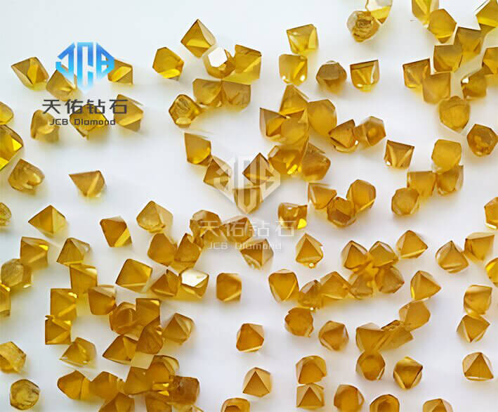
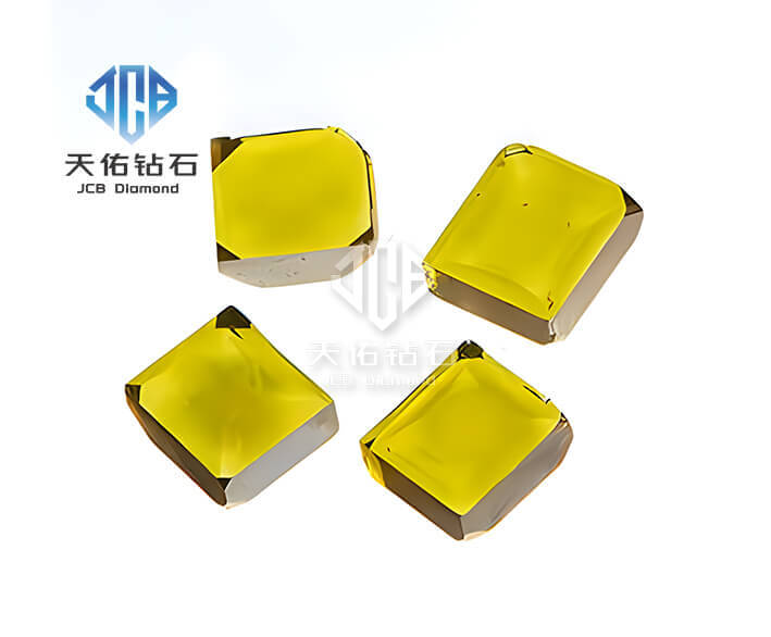
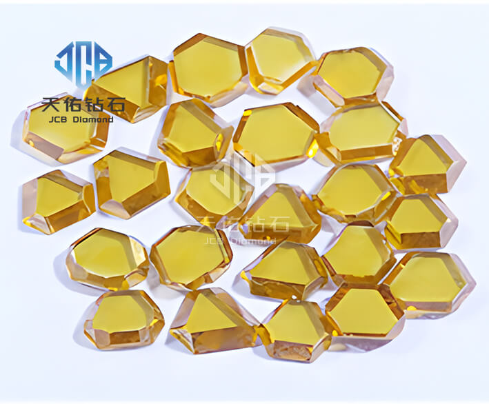
Thin diamond films are grown on a Si substrate using microwave plasma chemical vapor deposition (MPCVD). Diamond films of varying thickness can be obtained by controlling the growth time. First, an edge is scratched on the backside of the silicon wafer using a scribe pen, exposing the diamond-substrate interface. This exposed edge is crucial for exfoliating large, intact diamond films. By applying transparent tape to the top of the film and stretching it along the cut edge, a complete 2-inch diamond film with a thickness of 1 μm can be exfoliated. Optical imaging tests demonstrated that the resulting 2-inch diamond film exhibited excellent optical transparency and structural integrity. Furthermore, diamond films of varying thicknesses (200-800 nm) could be exfoliated. Compared to existing work dating back 30 years, this study represents the first large-scale production of wafer-scale diamond films.
In addition, commercially available diamond films grown on Si or Mo substrates can also be exfoliated using this method. After dissolving the tape in piranha solution (a mixture of concentrated sulfuric acid and 30% hydrogen peroxide (7:3)), the isolated diamond film can be integrated onto various substrates, including GaN, MoS2, and flexible PDMS, demonstrating the broad application potential of this method.
Diamond Film Properties and Applications
This edge-exposed exfoliation method allows for the rapid and simple preparation of transferable, wafer-scale diamond films, resulting in ultra-flat and ultra-thin diamond films. Experimental results indicate an optimal exfoliation window, and theoretical analysis provides guidance for the fabrication of industrial products. Furthermore, this method is scalable and compatible with various thicknesses and sizes. Unlike single-crystal bulk diamond, this diamond film exhibits similar optical properties (refractive index of 2.36 at 450nm), thermal conductivity (1300 W m⁻¹ K⁻¹), and resistivity (10⁻¹Ω). Unlike other methods, the resulting diamond film exhibits excellent flatness (roughness <1nm), making it suitable for delicate micro- and nanofabrication processes. The diamond film is strain-tolerant (up to 4% stress), and centimeter-scale diamond films exhibit macroscopic elastic strain. This holds promise for next-generation diamond electronics (field-effect transistors, p–n junction diodes), photonic devices (Raman lasers, UV detectors, metal lenses and planar photonic devices based on metasurfaces, photonic structures with ring and cavity resonators, waveguides, nanopillars), mechanical devices (e.g., mechanical cantilevers, microelectromechanical systems), thermal devices (on-chip heat sinks), acoustic devices (surface acoustic wave filters, planar acoustic metamaterials), and quantum technology devices (scalable and customizable devices).