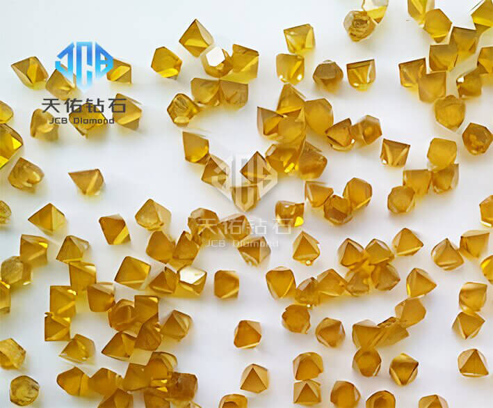
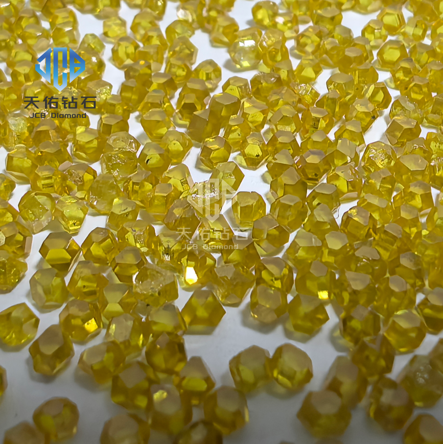
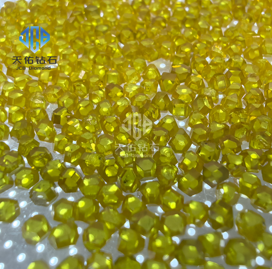
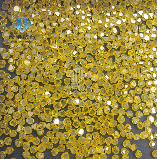
The JCB JLD Large Single Crystal Diamond series represents a significant advancement in synthetic diamond technology, comprising monocrystalline diamonds exceeding 1.0 mm in diameter. Fabricated under precisely controlled high-temperature and high-pressure (HPHT) conditions, these diamonds exhibit a hexoctahedral crystal morphology, exceptional purity, and uniform optical transparency. With superior static pressure strength, impact toughness, thermal resilience, and abrasion resistance, this product line serves as a critical material in high-precision industrial applications.
Key Material Characteristics and Synthesis Innovations
Exceptional Physical Properties
Extreme Hardness: Demonstrating a hardness value over 50 times greater than tungsten carbide, tools integrated with JCB JLD diamonds achieve a 3–5 fold increase in operational lifespan under high-load machining conditions.
Superior Thermal Conductivity: Offering thermal conductivity within the 1800–2200 W/(m·K) range—five times that of copper—these diamonds effectively manage heat dissipation in high-power electronic systems.
Anisotropy Optimization: Precise crystallographic orientation allows for micro-level cutting edge fabrication, achieving edge radii as fine as 0.002 μm through controlled directional processing.
Manufacturing Technology Advances
HPHT Synthesis: China's leading φ850mm press systems now deliver 60-carat single-cycle yields, with energy consumption reduced to 2200 kWh per 10,000 carats.
CVD Development: Domestic MPCVD reactors attain deposition rates exceeding 10 μm/h while maintaining consistent thermal conductivity ≥1800 W/(m·K), enabling mass production of 4-inch single-crystal wafers.
Cross-Industry Application Practices
1. Direct Applications and Production
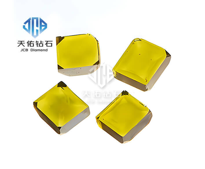
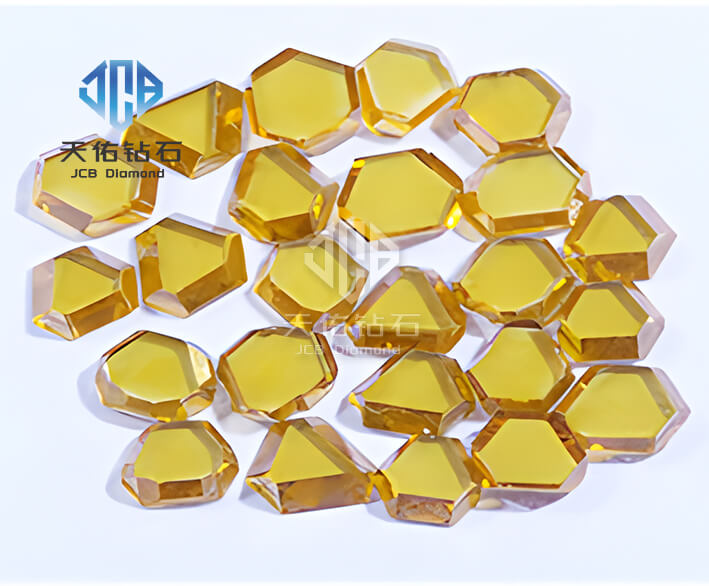
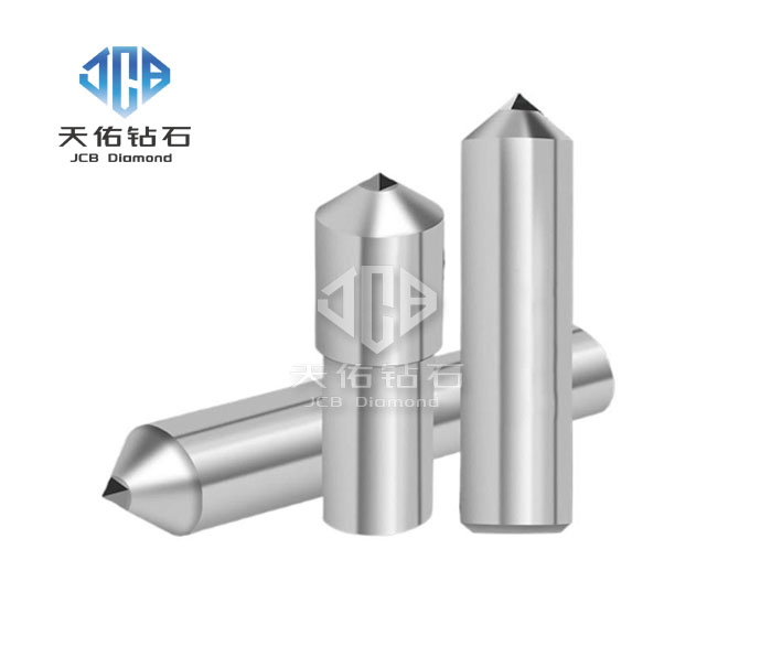
Large single crystal diamonds can be directly fabricated into single-point dressing tools, multi-point dressing tools, diamond grinding wheels, single crystal wire drawing dies, diamond rollers and so on. When cut along the {100} plane, they can be processed into diamond single crystal substrates, while cutting along the {111} plane produces ideal wire drawing die cores. As a versatile raw material for numerous diamond products, large single crystal diamonds offer remarkable cost-effectiveness, significantly reducing production expenses while enabling enhanced quality control.

2. Precision Machining & Tooling
Ultra-Precision Cutting Tools: Deployed in aerospace component fabrication for gyroscopes and laser reflector surfaces, achieving sub-nanometer surface roughness.
Energy Sector Drill Tools: PDC cutters enhanced with large-diamond composites demonstrate 30% improvement in impact resistance, extending service life fivefold in hard rock formations.
Abrasive System Integration: JLD series abrasives facilitate precision stone processing and ceramic honing operations across 18/20 to 500/600 mesh specifications.
3.Semiconductor & Thermal Management
Advanced Thermal Solutions: CVD diamond heat sinks successfully address thermal fluxes exceeding 500 W/cm² in GaN/SiC power devices, with verification from industry leaders including Huawei and Infineon.
Wafer Processing Enhancement: Ultra-Premium Micron Diamond (UPM) powders with ±5% size distribution enable silicon wafer thinning to Ra<0.5 nm, increasing production yield by 15%.
Quantum Technology Enablers: Nitrogen-vacancy center diamonds facilitate quantum magnetoencephalography applications with spin coherence durations surpassing 2 ms.
4.Next-Generation Energy Systems
Electric Vehicle Components: Implementation in 800V platform motor cooling systems and LiDAR windows reduces thermal resistance by 40%.
Aerospace Manufacturing: Cutting tools maintain operational effectiveness three times longer than conventional solutions when processing challenging TiAl alloys.
Fuel Cell Innovation: Nano-diamond supported Pt-Ti catalysts demonstrate 50% greater activity compared to standard Pt/C formulations.
5.Specialized Components & Optical Systems
High-Power Laser Applications: Nano-diamond coatings provide >95% transmittance in vacuum window applications, superseding polished CVD alternatives.
Precision Mechanical Systems: Nano-diamond lubricants establish "ball-bearing structural films" that reduce friction coefficients by twenty times.
Global Market Dynamics and Development Trends
Current Industry Landscape
China maintains dominant production capacity, accounting for ≥95% of global output with 2024 projected industry value surpassing RMB 17 billion. However, semiconductor-grade CVD equipment localization remains below 20%, with high-purity ≥4-inch electronic-grade crystals still predominantly supplied by Japanese (Sumitomo) and European (Element Six) manufacturers.
Strategic Development Pathways
Technology Scaling: 6-inch CVD single-crystal development road map (2025-2030) projects 15% annual cost reduction.
Sustainable Manufacturing: HPHT synthesis transition to 100% renewable energy sources outperforms EU carbon standards by 30%.
Global Standardization: China-led ISO "Single-Crystal Diamond Heat Spreader" standardization initiative expected to increase high-value export share to 55% by 2030.
Competitive Challenges and Strategic Recommendations
Technical Barriers
Maintaining crystal defect densities below 5×10¹³ cm⁻³ requires breakthroughs in CVD epitaxial control methodologies.
Cooperative Development Models
Strategic partnerships with precision tool manufacturers (e.g., Waldon Ultra-Precision Tools) enable development of application-specific solutions.
Intellectual Property Management
Targeted acquisition of CVD patent portfolios through international mergers and acquisitions establishes comprehensive "defensive-litigation" capabilities.
Industry Outlook
Large single crystal diamond technology continues its transition from conventional industrial abrasive applications toward functioning as an enabling material for advanced manufacturing, semiconductor, and quantum technology sectors. With continued advancement in high-performance, environmentally sustainable synthesis techniques, this material category demonstrates significant potential for multibillion-dollar market expansion in the coming decade.