With the rapid advancement of electronic devices toward miniaturization, multifunctionality, high power consumption, and enhanced reliability, high-density three-dimensional integration technology for microelectronic devices has emerged. However, the development of high-density integration is constrained by elevated junction temperatures caused by thermal concentration within chips, significantly compromising device performance and reliability.

Integrated chips feature multi-layer structures comprising substrate layers, chip circuit layers, chips, and package shell cold plates. The package shell cold plate incorporates microchannels that dissipate heat from the circuit layer chips via liquid convective heat transfer while ensuring uniform chip temperature distribution. Flexible thermal interface materials (TIM) bridge the interface between the package shell cold plate and the circuit layer.

Thermal interface materials (TIMs) are critical heat dissipation components that fill microscopic gaps between surfaces to directly enhance thermal performance. TIMs are typically applied between the chip and package lid (TIM1), chip and heat sink (TIM1.5), and package lid and heat sink (TIM2). High thermal conductivity and reliability in TIMs ensure rapid heat transfer across interfaces. The prevailing thermal management approach for high-computing-power chips still relies on ultra-low thermal resistance TIM1 materials to rapidly conduct heat from the chip interior to the package housing. Heat is then transferred via TIM2 materials to a liquid cooling plate, which rapidly dissipates it to the external environment through the rapid flow of its internal cooling fluid.

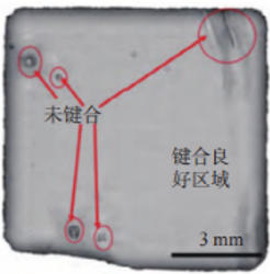
Additionally, low-temperature bonding techniques have gained widespread adoption in packaging processes. For instance, low-temperature Cu-Cu bonding has become a core technology in advanced packaging due to its advantages in high-density interconnects and excellent electrical and thermal conductivity. The nano-silver sintering process exemplifies low-temperature bonding technology. It forms connection interfaces with high thermal conductivity (250 W/(m·K)) at low temperatures (250°C), effectively avoiding thermally induced damage associated with traditional high-temperature processes. The resulting connection structures exhibit extremely low porosity, outstanding thermal conductivity, and exceptional mechanical stability, providing reliable assurance for advanced packaging.


