Thermal Management: The “Invisible Ceiling” of the High-Power Era
As AI chip power consumption crosses the kilowatt level, the heat flux density of millimeter‑wave power amplifiers in 6G base stations exceeds 300 W/cm², and the local temperatures of SiC modules in new‑energy vehicle high‑voltage platforms rise sharply. Conventional thermal materials are approaching their physical limits. Thermal management is no longer a “supporting process” but has become a core bottleneck that constrains performance delivery.
Pure copper has a thermal conductivity of about 400 W/(m·K), aluminum only 237 W/(m·K), and thermal interface materials like thermal greases are only 0.8–3 W/(m·K). Faced with local heat flux densities exceeding 1000 W/cm² in AI chips, traditional solutions are increasingly inadequate. Chip overheating leads to frequency throttling, loss of computing power, shortened lifespan, and even direct burn‑out – these are challenges that every high‑power‑density scenario must confront.
Copper‑diamond (Cu‑diamond) composites have thus entered the industrial spotlight. They combine the ultra‑high thermal conductivity of diamond with the good workability of copper. The theoretical thermal conductivity reaches 2000–2200 W/(m·K), while mass‑produced products typically achieve 600–800 W/(m·K). The coefficient of thermal expansion (CTE) can be precisely tuned to 5–7×10⁻⁶/K, matching perfectly with gallium arsenide, indium phosphide, and silicon‑based semiconductors. This material is regarded by the industry as one of the “ultimate solutions” for next‑generation thermal management, and 2026 has become the critical year for its large‑scale application.
Copper‑Diamond: How to Achieve “1+1>2”?
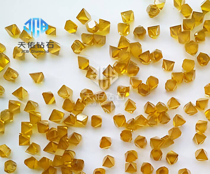
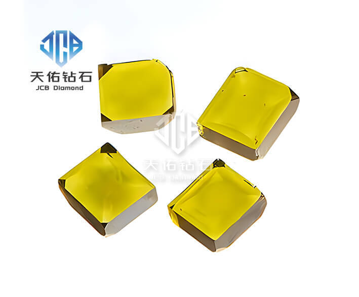
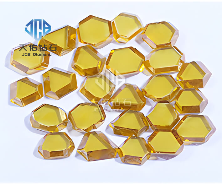
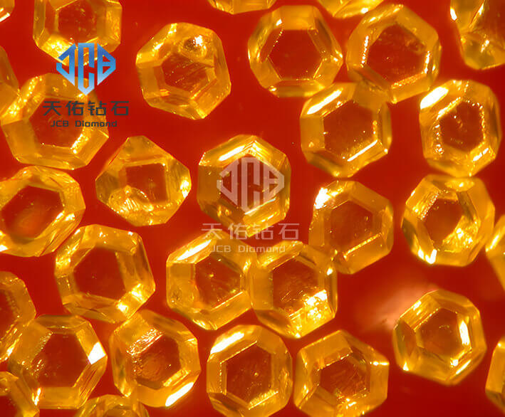
The copper‑diamond composite consists of a copper matrix and diamond reinforcement. Diamond is one of the materials with the highest known thermal conductivity – type IIa diamond has a theoretical value of 2000–2200 W/(m·K), more than five times that of pure copper. However, copper and diamond are naturally “incompatible” – at high temperatures, the wetting angle of copper on diamond approaches 150°, meaning almost no wetting occurs. Direct mixing produces numerous micro‑gaps and extremely high interfacial thermal resistance. After more than a decade of industry iteration, a core interface modification approach based on “surface metallization” has emerged: coating the diamond surface with transition metals such as titanium or chromium to form a stable carbide interlayer, converting physical contact into chemical bonding. After treatment, the interfacial thermal resistance can be reduced by more than two orders of magnitude, truly unlocking diamond’s thermal conduction potential.
The final performance of copper‑diamond is determined by the volume fraction, particle size, and distribution uniformity of the diamond. In mass production, the diamond volume fraction is typically in the range of 40%–70%. According to industry surveys, 50%–60% offers a good balance of overall properties, delivering stable thermal conductivities of 600–800 W/(m·K), with some high‑end products exceeding 1000 W/(m·K). The CTE can be precisely controlled within 5–7×10⁻⁶/K by adjusting the parameters, closely matching chip materials such as gallium arsenide, indium phosphide, and silicon‑based semiconductors, effectively mitigating interface warpage and failure risks during thermal cycling.