The stability of metal wire diameter tolerances at the micrometric level does not depend on large-scale industrial equipment, but rather on the single die through which the wire passes. Polycrystalline diamond (PCD) wire drawing dies are critically important in this process because their material structure and manufacturing technology jointly establish a fundamental threshold for both precision and service life. This article addresses key technical questions concerning PCD wire drawing dies.
The Starting Point of PCD Core: Engineered Diamond Micropowder and Sintering Technology
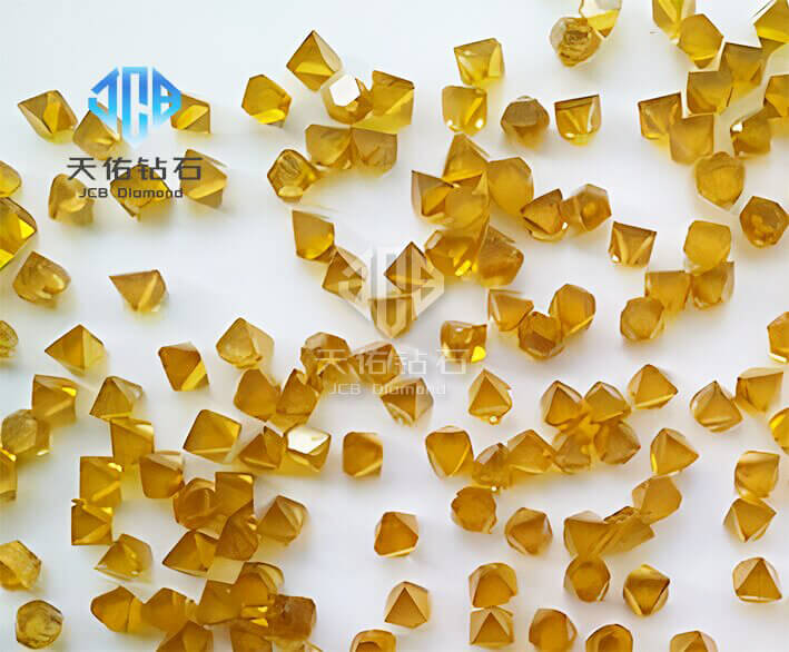
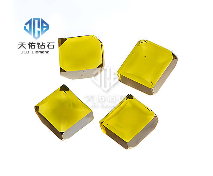
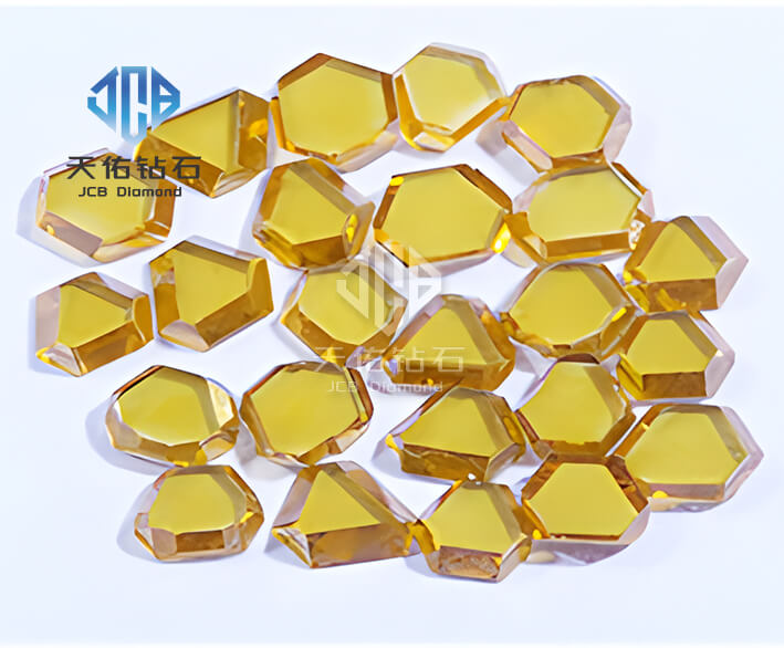
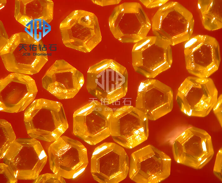
The foundation of a PCD core begins with carefully selected synthetic diamond micropowder. When these micropowders are mixed with binders such as cobalt and silicon and sintered under high temperature and high pressure conditions, direct bonding forms between the diamond particles, enabling the polycrystalline aggregate to simultaneously possess hardness and wear resistance approaching that of natural diamond, along with favorable thermal conductivity. The selection of binder is not inconsequential: cobalt-based PCD exhibits superior machinability and is suitable for most conventional wire-drawing operations; silicon-based or thermally stable PCD, conversely, maintains structural integrity at elevated temperatures and is oriented toward wire-drawing scenarios sensitive to thermal loading.
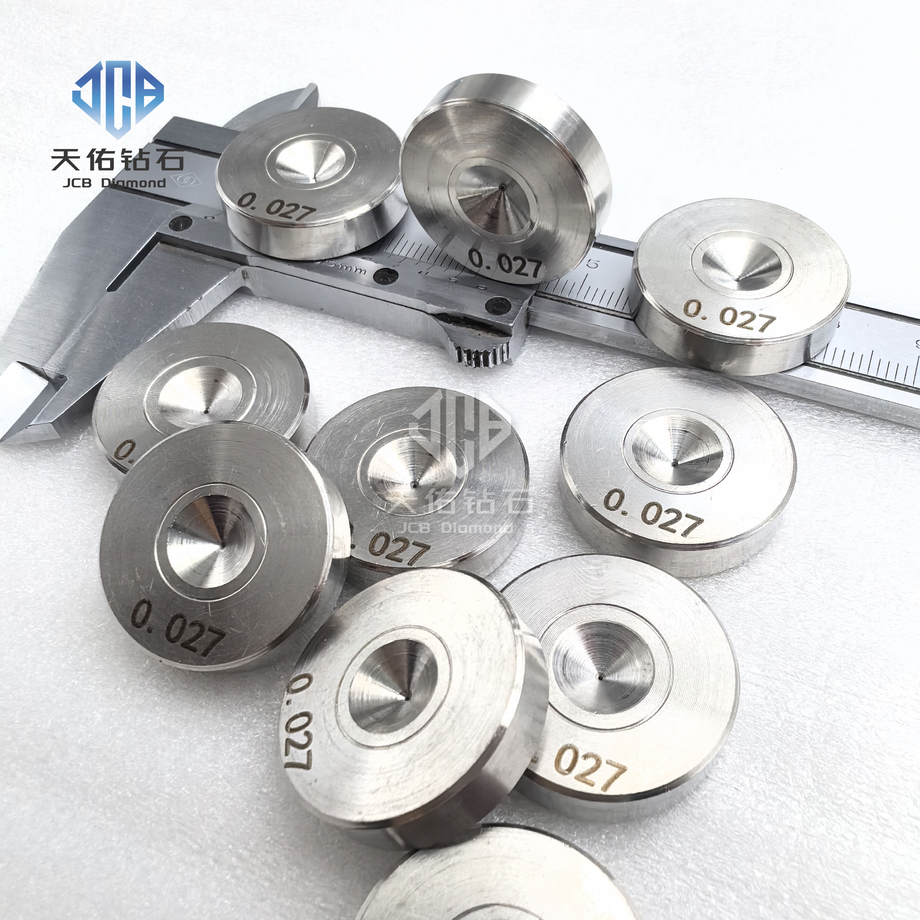
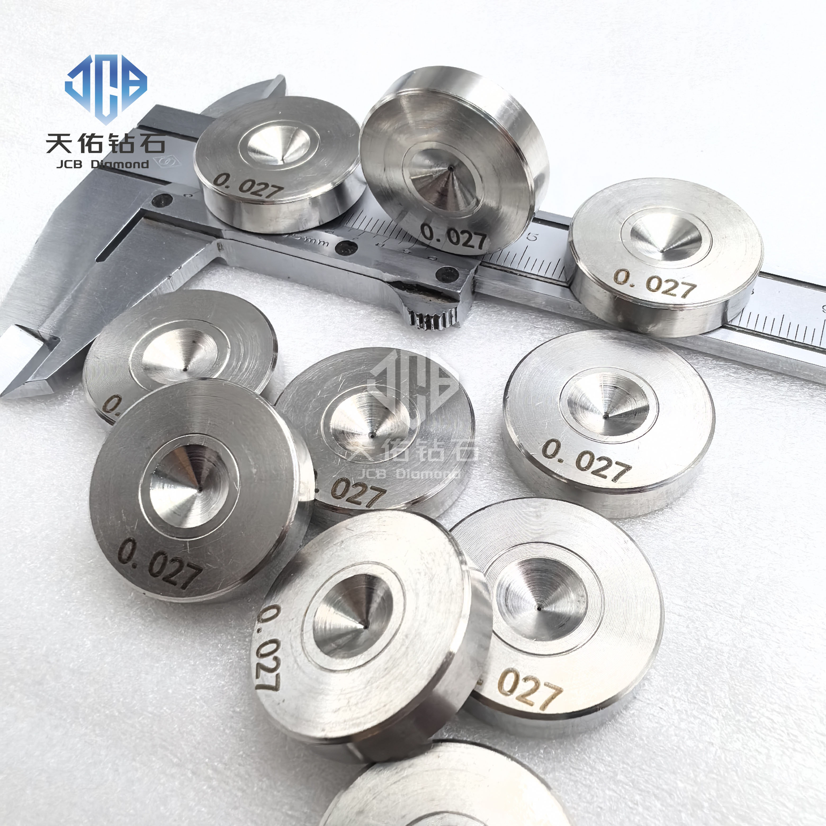
Die Orifice Formation: Laser Perforation Determines Feasibility; Polishing Determines Quality
The central orifice of the die core represents the functional nucleus of the entire die, with its formation pathway constrained by the material's electrical conductivity. Cobalt-based PCD containing metallic phases exhibits electrical conductivity and can be efficiently formed through electrical discharge machining (EDM) or wire electrical discharge cutting (WEDM); electrically insulating PCD typically requires laser drilling instead. In industrial practice, laser perforation serves as a "rough forming" operation: it initially establishes the approximate orifice diameter and the angle of the compression zone, while leaving adequate stock for subsequent precision machining.
The actual transition of the die orifice into the usable precision range is accomplished by the finishing and polishing operations that follow. The typical manufacturing sequence, after laser perforation, employs specialized shaping equipment to machine the entrance, compression zone, sizing zone, and exit zone to specified geometric profiles and angles. Subsequently, ultrasonic lapping combined with ultra-fine diamond abrasive powder polishes the inner wall of the sizing zone to achieve the required surface roughness and wire diameter precision. Surface quality of the sizing zone constitutes a critical specification: certain high-precision wire drawing die patents stipulate that the roughness (Ra) of this region shall not exceed 0.05 μm, a dimensional range directly correlated with the surface finish and roundness consistency of the drawn wire. In essence, laser perforation determines whether die orifice formation is feasible, whereas grinding and polishing determine whether it can reliably produce conforming wire.
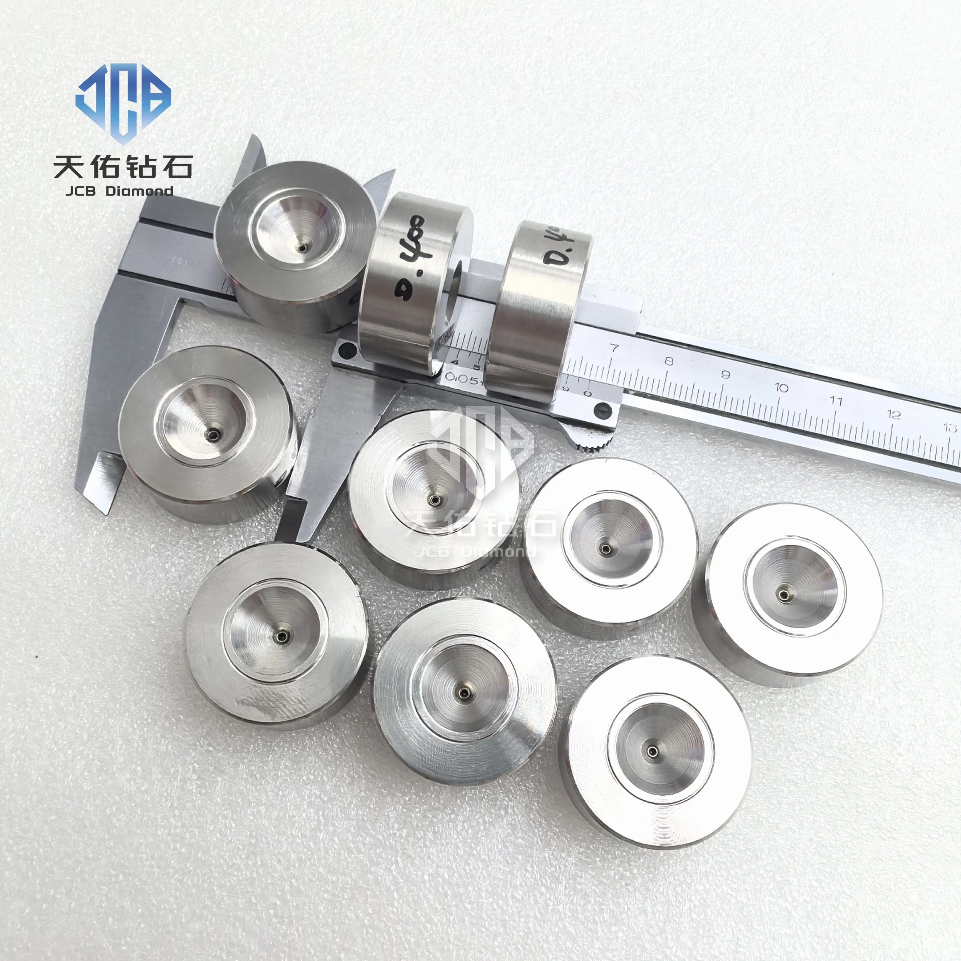
Application Landscape of PCD Wire Drawing Dies
The application landscape of PCD wire drawing dies can be understood along two principal trajectories. The first represents the foundational domain of conventional metal wire manufacturing. In the electrical wire and cable sector, the drawing of copper wire, aluminum wire, and high-voltage, medium-voltage, and low-voltage cable conductors constitutes one of the most stable and reliable demand sources for PCD dies; in the steel wire products sector, steel cord, coated steel wire, stainless steel wire, and welding wire (including gas metal arc welding wire and flux-cored arc welding wire) similarly depend on PCD dies to maintain wire diameter consistency and surface quality over extended operating periods. The core requirements imposed by these applications are wear resistance and service life; the randomly oriented polycrystalline diamond grain structure of PCD causes die orifice wear to proceed uniformly, thereby facilitating wire roundness maintenance and minimizing ellipticity drift.
The second trajectory encompasses the incremental market defined by precision manufacturing and emerging applications. Semiconductor bonding wire represents one of the most demanding scenarios: gold wire, copper wire, and aluminum wire in packaging interconnection require extremely fine wire diameter and exceptional surface integrity, where the roundness retention capability and surface roughness control of PCD dies are irreplaceable. Silicon wafer cutting wire represents an opposite extreme for PCD wire drawing dies: cutting wire diameter continues to evolve toward finer specifications, with tungsten-diamond wire now established in the 20–22 μm diameter range as the mainstream, and even finer specifications still undergoing developmental trials. With each incremental reduction in wire diameter, the requirements for die orifice precision and wear stability advance correspondingly. Additionally, copper wire for automotive high-voltage harnesses, medical guidewires, superconducting wire, and precious metal wire drawing are progressively redefining PCD dies from "wear-resistant tools" to "precision assurance components."