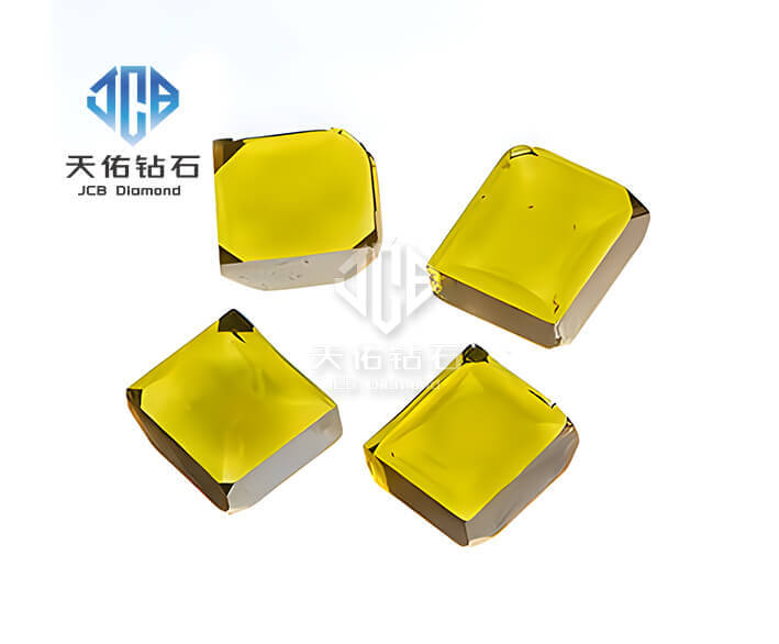
Power Diamond Systems, founded at Waseda University, has successfully developed a diamond MOSFET with a 550 V blocking-voltage rating and a drain current of 0.8 A. It has also demonstrated switching at 200 V and 1 A for the first time. This is an important milestone on the path toward the practical application of diamond power semiconductors.
Diamond semiconductors have outstanding physical properties, including a wide bandgap and a high dielectric breakdown field strength. They are considered an important material for next-generation power devices. However, a technical challenge remains before they can be put to practical use: increasing the voltage withstand capability while simultaneously reducing on-resistance.
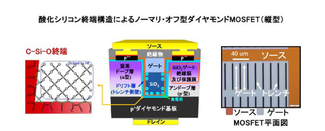
In particular, in high-voltage device designs, electric-field concentration can easily occur at the gate edge, limiting the device’s ability to withstand voltage between the drain and source. In addition, increasing current capacity has often required connecting multiple small devices in parallel to achieve a higher output current.
To address these challenges, Power Diamond Systems built on its core diamond MOSFET technology and introduced a “field plate” structure. This design effectively spreads and reduces electric-field concentration at the gate edge, thereby increasing the device’s voltage withstand capability.
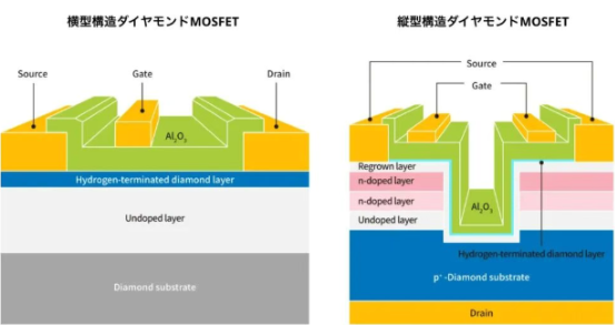
The research team also developed a design with a larger device area, enabling a single device to carry more current. This makes high-current operation possible without connecting multiple small devices in parallel.
The results of this research are expected to help advance the practical application of diamond power semiconductors in high-efficiency power electronics systems.