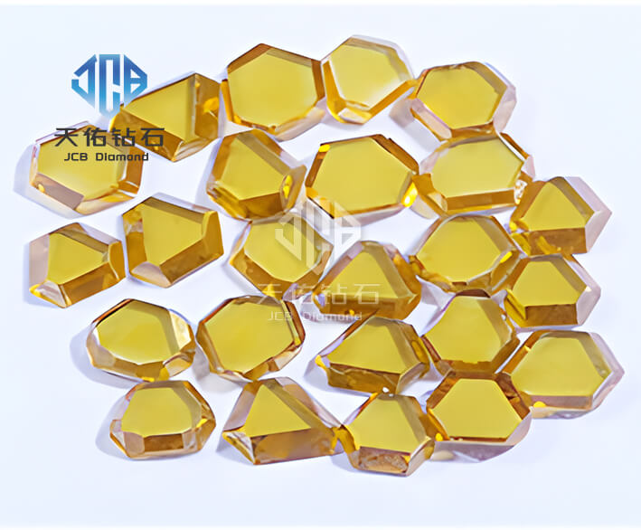
ecently, domestic superhard material manufacturers have continued to upgrade production lines and carry out customer validation for CVD diamond heat sinks (diamond thermal spreaders). Multiple models of large-size polycrystalline CVD diamond heat sinks have entered small-batch delivery. These products target high-end markets including AI computing chips, radio frequency devices, high-power lasers and silicon carbide power modules, delivering a domestically sourced core material solution for thermal management of high-power electronic equipment.
CVD diamond heat sinks are fabricated via chemical vapor deposition. Their room-temperature thermal conductivity reaches 1800–2200 W/(m·K), 4 to 5 times that of pure copper. They also feature a low coefficient of thermal expansion, excellent electrical insulation and high-temperature stability. These heat sinks rapidly equalize local hotspots on chips, lower the peak temperature of components and extend the service life of high-power chips and lasers, making them a well-recognized high-performance thermal spreading material in the advanced thermal management sector. As power consumption rises for servers running large AI models, automotive power semiconductors and satellite communication RF devices, traditional copper and aluminum heat dissipation materials are gradually hitting physical limits, and demand for CVD diamond cooling solutions is growing rapidly.
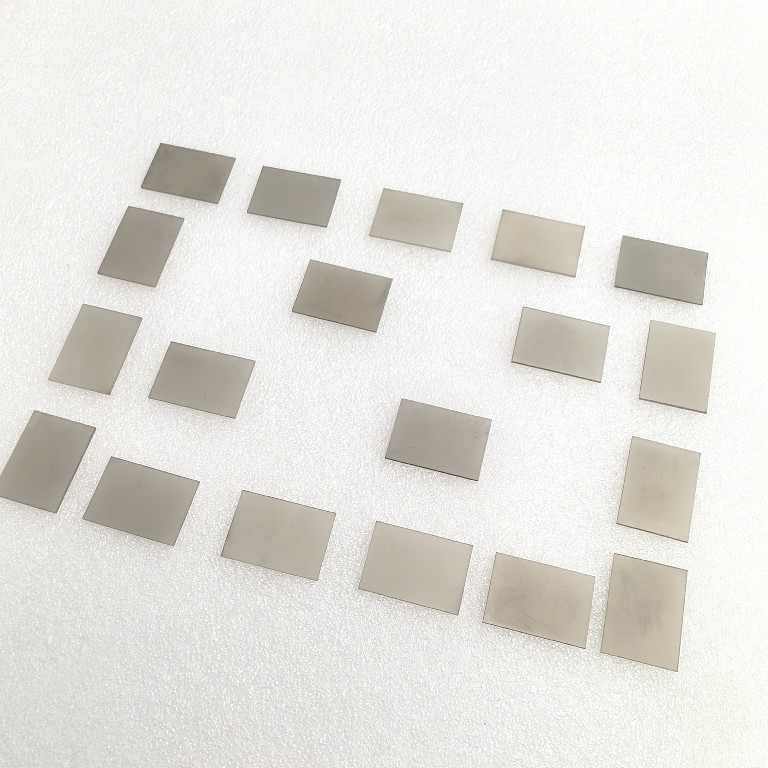
It is reported that China has established a complete industrial process chain covering MPCVD deposition, precision lapping, metallization and profile cutting. Breakthroughs have been achieved in mass production of 8-inch large-size CVD diamond heat sinks, with yield rates continuously optimized. This reverses the previous situation where high-grade diamond thermal spreaders relied heavily on overseas supply. The products support single-sided or double-sided metallization and can be directly bonded to chips, laser bars and RF chips during packaging. They are suitable for multiple scenarios including package-level heat spreading and module cooling. At present, samples have been submitted for reliability verification to leading customers in computing, optoelectronics and power semiconductor industries, and certain models have secured steady trial orders.
Industry insiders point out that the core value of CVD diamond heat sinks lies in solving hotspot issues under ultra-high heat flux density. Every 10 ℃ reduction in a chip’s hotspot temperature greatly improves device reliability, allows computing hardware to stably run at higher performance levels and cuts cooling energy consumption in data centers. Compared with diamond-copper composites, pure CVD diamond heat sinks offer a higher thermal conductivity ceiling and superior insulation, making them suitable for harsh operating conditions in lasers, RF devices and aerospace equipment. Diamond-copper composite solutions are more oriented toward large-scale commercial adoption in AI servers, and both technical routes are developing in parallel.
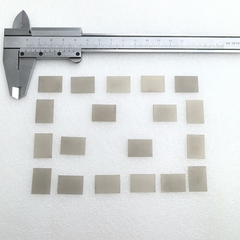
At present, China’s superhard material industrial clusters are actively expanding production capacity. Multiple enterprises are adding new CVD equipment to drive down manufacturing costs for large-size diamond heat sinks. This pushes the products from research and small-batch special applications toward mass markets such as AI servers and automotive power semiconductors. Going forward, with further cost reduction and mature supporting packaging processes, CVD diamond heat sinks are expected to become a core material for next-generation high-end electronic thermal management and support the independent and controllable development of China’s computing, optoelectronic and third-generation semiconductor industrial chains.