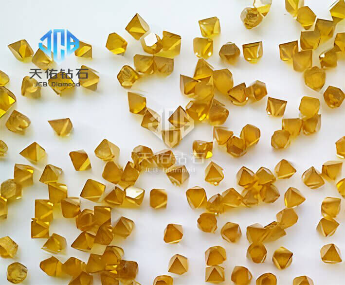
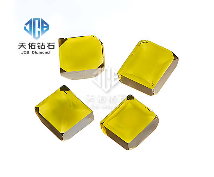
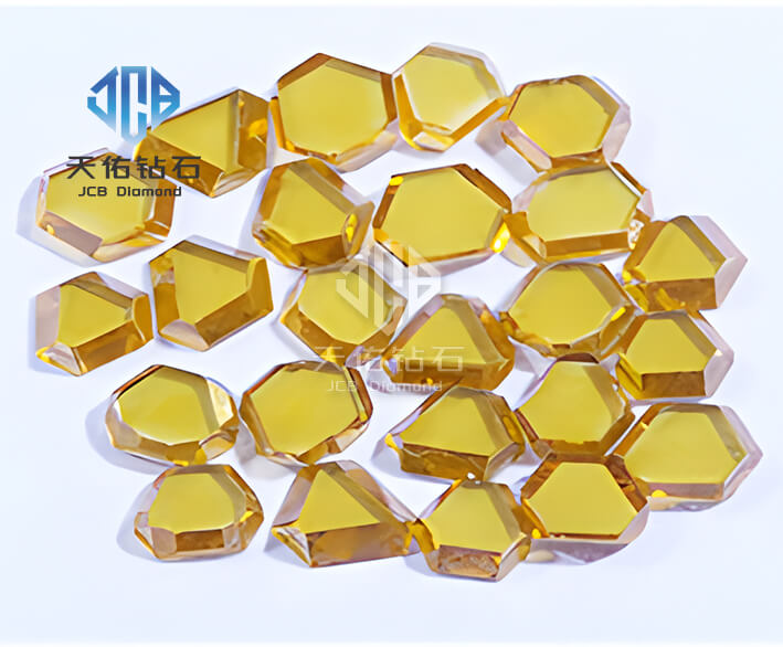
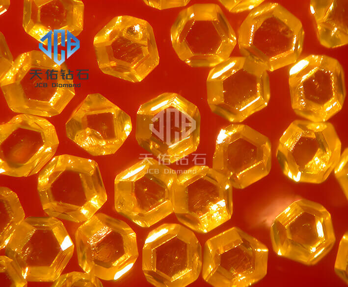
As domestic superhard material enterprises continuously advance process iteration and large-scale verification of CVD diamond heat sink wafers, the diamond heat dissipation substrates prepared via Chemical Vapor Deposition technology, boasting ultra-high thermal conductivity, have become core materials for breaking the heat dissipation ceiling in AI computing chips, radio frequency devices, high-power lasers and third-generation semiconductors. The independent development of the domestic industrial chain keeps picking up speed.
With the explosive demand for large models, power consumption and heat flux density of high-end GPUs, SiC/GaN power devices keep climbing. Traditional heat dissipation materials such as copper, aluminum and aluminum nitride have gradually hit physical limits. The thermal conductivity of ordinary pure copper is about 400 W/m·K, while high-quality CVD diamond can reach 2000–2200 W/m·K, more than five times that of copper. Meanwhile, it features electrical insulation, low coefficient of thermal expansion and high stability. It can quickly dissipate local hot spots on chips and avoid short-circuit risks, meeting the strict requirements of high-density packaging scenarios.
According to industry technicians, CVD diamond is manufactured by the MPCVD (Microwave Plasma Chemical Vapor Deposition) process. Carbon atoms are directionally deposited and grown on the substrate surface under a controlled atmosphere. It can be processed into heat sink sheets and heat dissipation substrates of different specifications as required. Compared with natural diamond, synthetic CVD diamond is easier to achieve large-size and high-purity mass production. It can also support metallization and patterning processing, directly matching the chip packaging chain to reduce interface thermal resistance and improve heat spreading capacity.
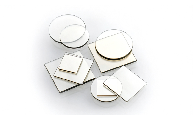
At downstream application ends, CVD diamond heat dissipation solutions have entered sample verification and small-batch delivery stages in multiple scenarios. In AI data centers, diamond heat spreaders are used for near-chip heat dissipation to ease hot spot accumulation of high-power GPUs and guarantee stable full-load operation of chips. In radio frequency, microwave and radar communication devices, diamond substrates can reduce thermal resistance of power amplifier components, raise output power and long-term reliability of high-frequency equipment. They are also gradually adopted in new energy power modules, industrial lasers and aerospace microelectronics to solve thermal failure problems under extreme working conditions.
On the industrial level, domestic research institutes and superhard material manufacturers keep tackling bottlenecks in equipment, growth technology and precision machining, gradually breaking overseas supply barriers for high-end diamond heat sink materials. The yield of large-size CVD diamond keeps rising while production costs keep falling. Multiple leading enterprises are expanding production simultaneously, promoting product standardization and serialization, and providing customized CVD diamond heat dissipation solutions for customers in semiconductor packaging, precision optics and power electronics.
Industry analysts believe thermal management has become a key shortcoming restricting the performance release of next-generation high-performance electronic devices. CVD diamond heat dissipation material is not a single heat dissipation accessory, but the base material for a new-generation thermal management system. As yield improves and cost keeps dropping, CVD diamond heat sink wafers will expand from high-end niche applications to large-scale popularization, laying a solid material foundation for computing infrastructure, third-generation semiconductors and advanced radio frequency industries, and serving as an important link for the development of new productive forces.