Key Performance Advantages
Exceptional Thermal Conductivity: Thermal conductivity at room temperature ranges from 1000 to 2200 W/(m·K), with custom grades available to meet specific requirements (TC1200, TC1500, TC1800, TC2000, etc.), far surpassing traditional heat dissipation materials such as copper and aluminum.
Excellent Electrical Insulation: With a resistivity as high as 10¹⁴–10¹⁶ Ω·cm, a dielectric constant of approximately 5.68, and a dielectric loss as low as 6.2×10⁻⁸, it can be directly bonded to the surface of active devices without the need for an additional insulation layer.
Low Thermal Expansion Matching: With a thermal expansion coefficient as low as 0.8–1.0 ppm/K, it is highly compatible with semiconductor materials such as Si, GaN, and GaAs, effectively resolving interface delamination issues caused by thermal mismatch.
High Mechanical Strength: Vickers hardness >8000 kg/mm², Young’s modulus 850–1100 GPa, tensile strength 450–1100 MPa. It is resistant to high temperatures and corrosion, enabling long-term stable operation in harsh environments.
Lightweight Design: With a density of only 3.52 g/cm³, it is lightweight, contributing to the miniaturization and portability of electronic devices.
Applications
AI Computing and Data Centers: Directly integrated into AI training chips and high-performance GPU/CPU packages, these solutions significantly reduce chip junction temperatures, effectively address “hotspot” issues under high heat flux densities (exceeding 1000 W/cm²), and enhance sustained high-load performance.
High-Power Semiconductor Lasers: Used as intermediate heat sinks for laser diodes and laser bars, significantly reducing thermal resistance. Application cases demonstrate that the thermal resistance of laser chips using diamond heat sinks is reduced by more than 81% compared to traditional ceramic substrates.
RF and Microwave Devices: Used in 5G/6G RF power amplifiers, TR modules, GaN-on-Diamond composite substrates, and more, enabling higher power density and higher-frequency operation, with thermal resistance reduced by approximately 30%.
Power Electronics and New Energy Vehicles: Used for heat dissipation in wide-bandgap power modules such as SiC and GaN, controlling temperature rise during charging and discharging, and improving power density and system reliability.
Aerospace and Defense: Used for thermal management in extreme environments, such as heat spreaders for satellite electronic systems, high-power radar components, and spacecraft electronics.
Optical Communications and High-Speed Interconnects: Used for cooling laser chips in 800G/1.6T optical modules, stabilizing wavelength and output power, and significantly reducing bit error rates.
Customization Services
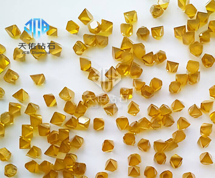
Our company possesses end-to-end manufacturing capabilities spanning the entire diamond production chain—from crystal growth to wafer fabrication, testing, and application—and offers one-stop customization services tailored to customer needs:
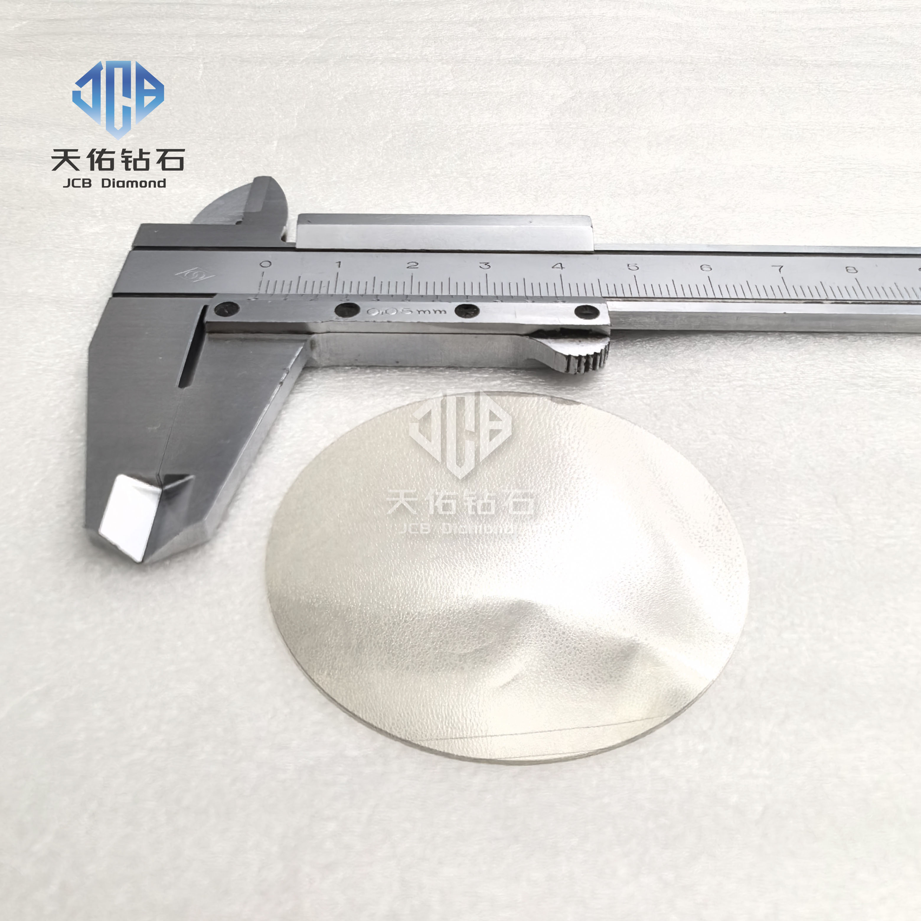
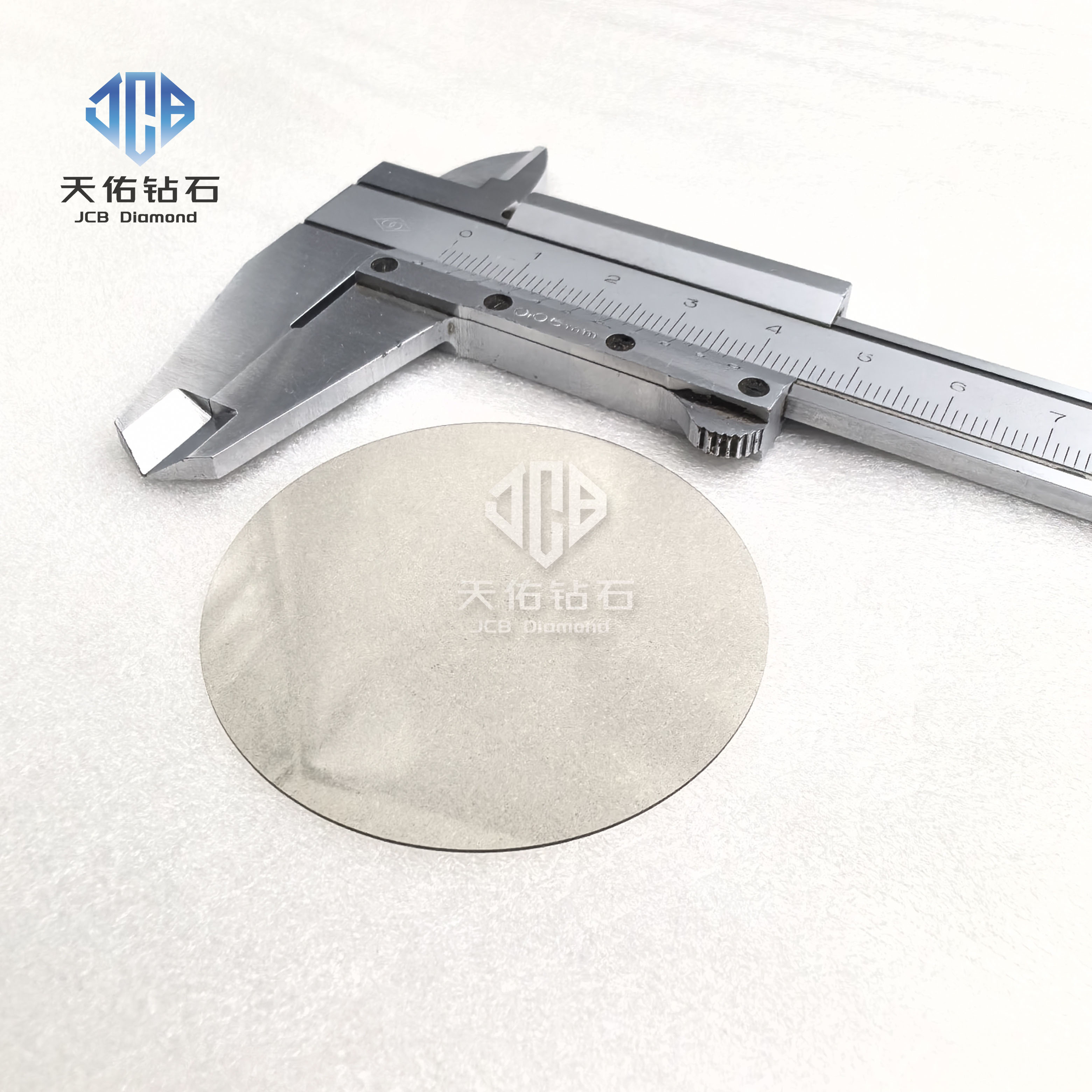
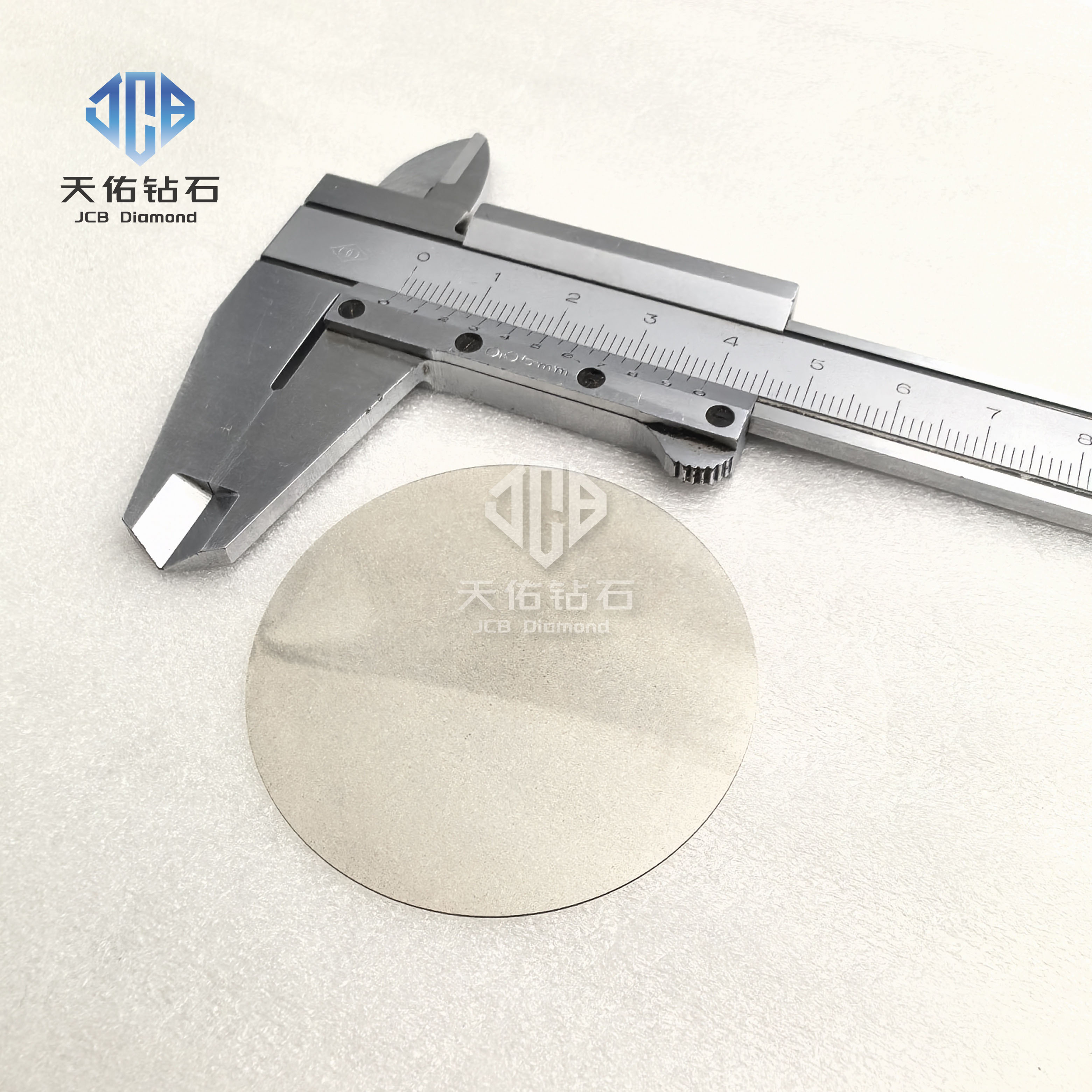
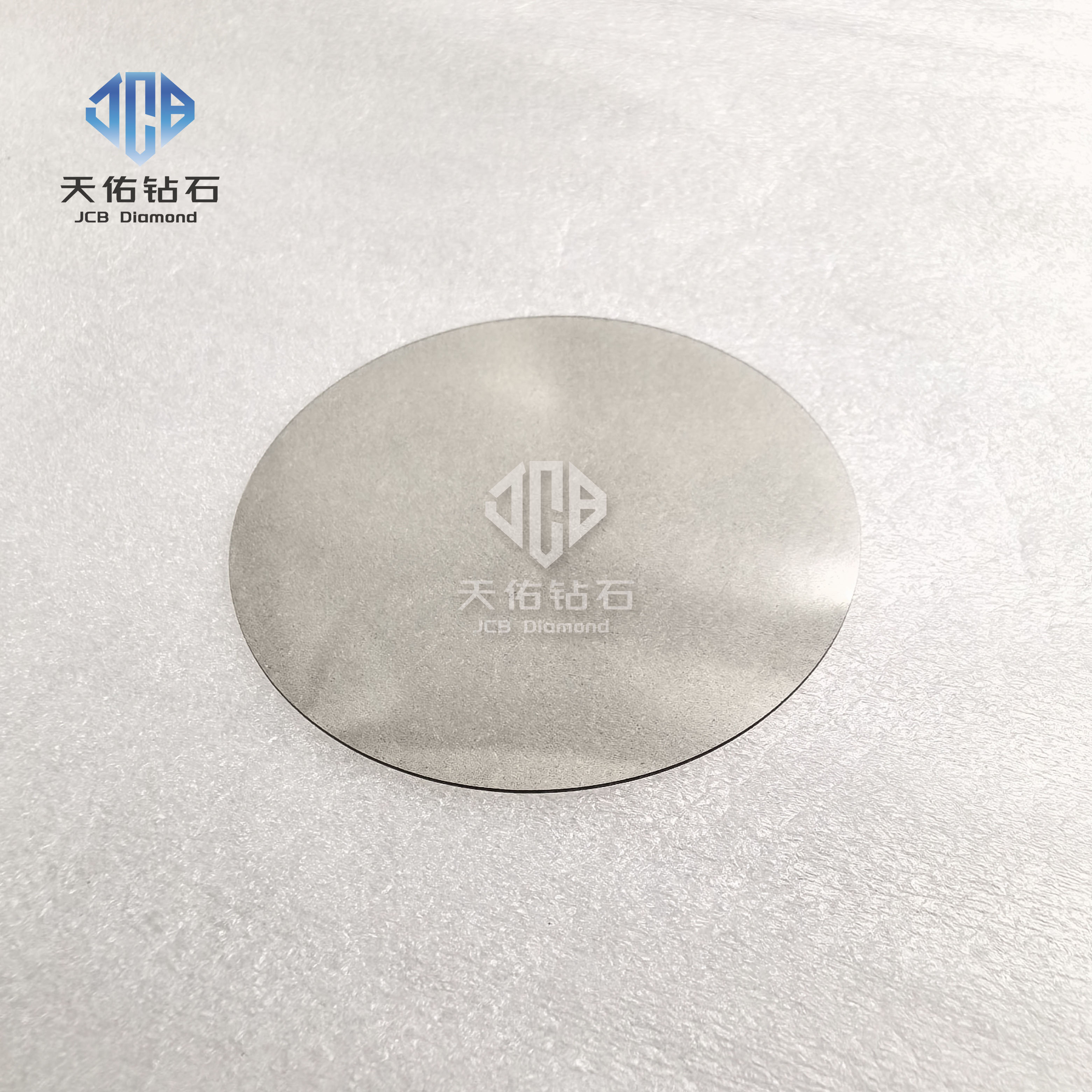
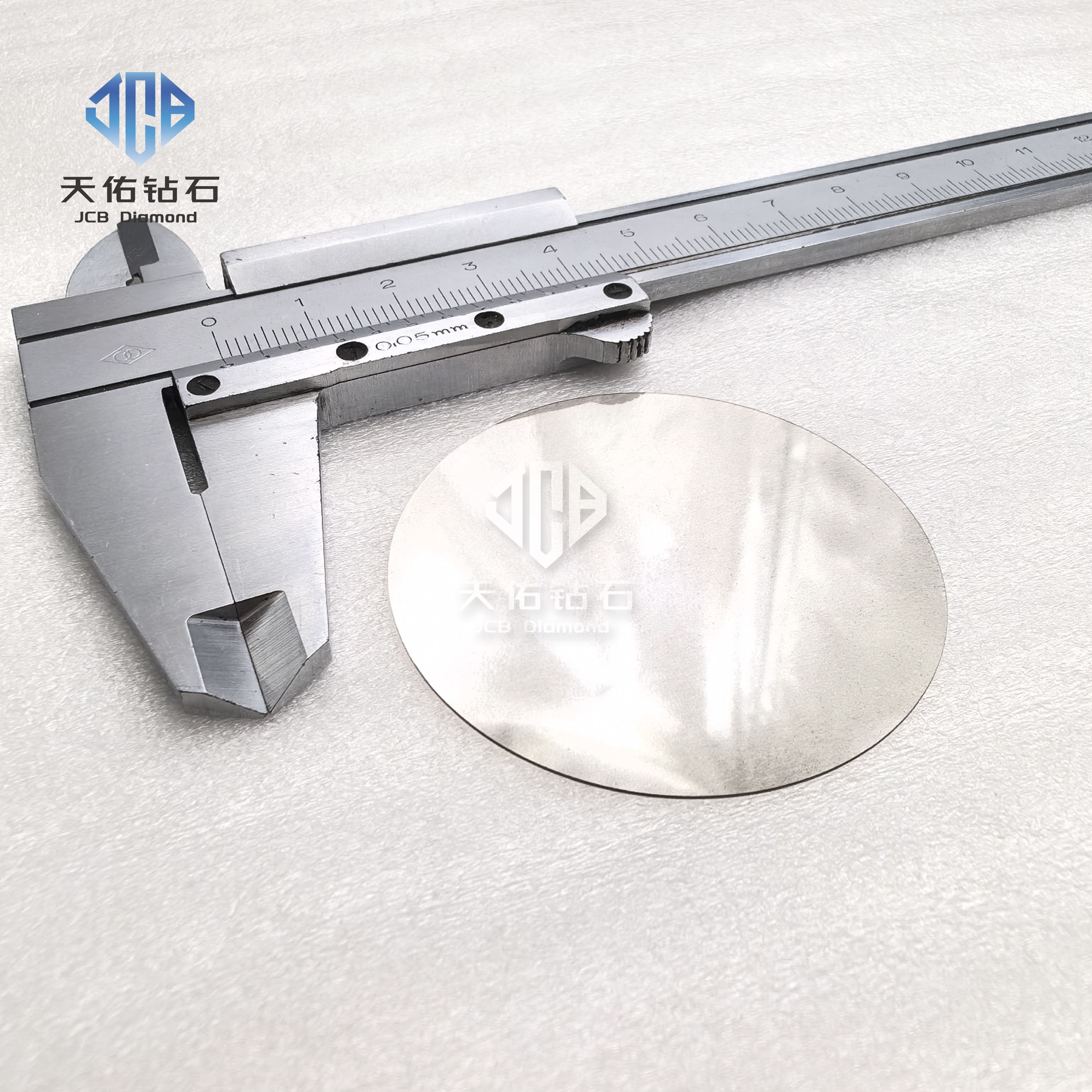
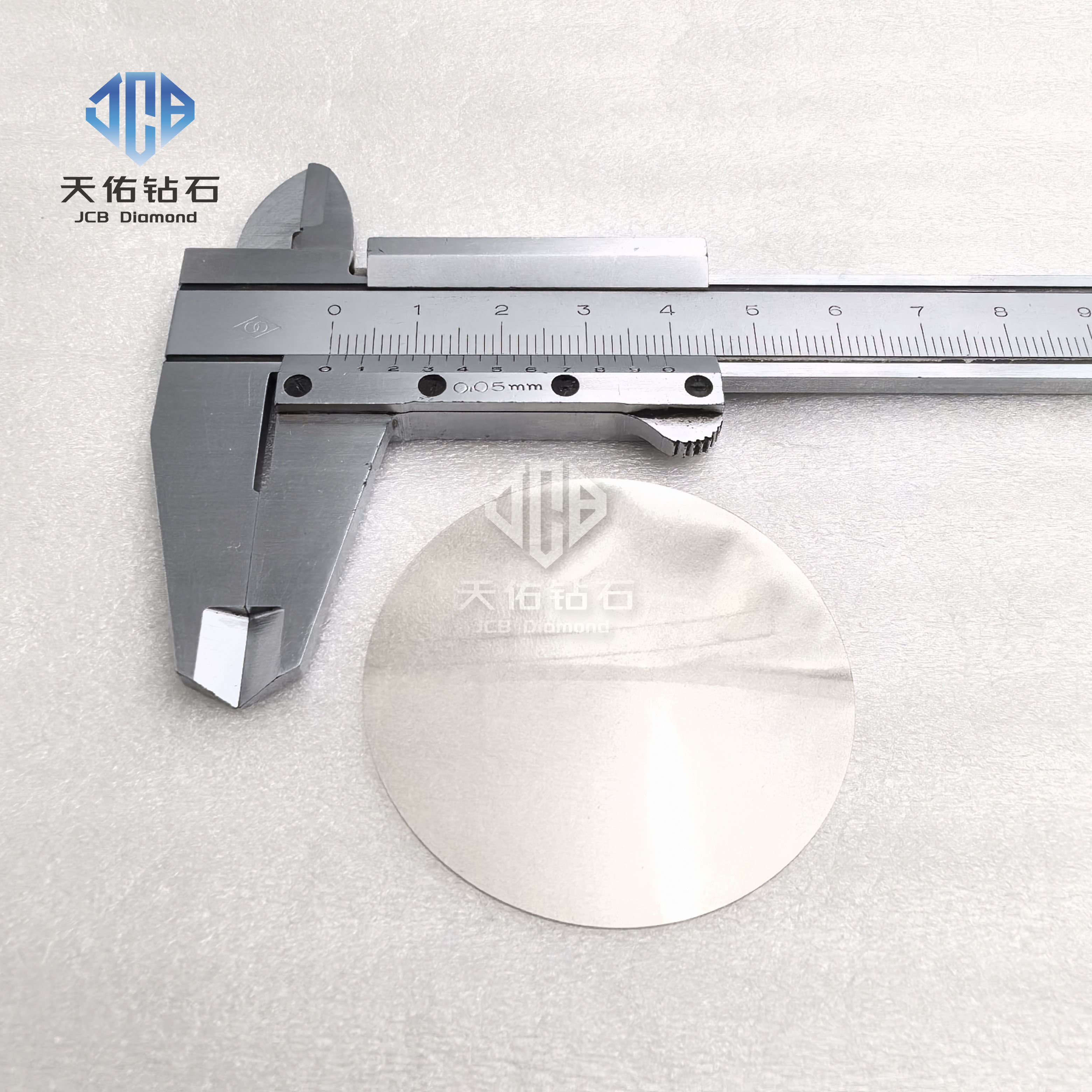
Custom Sizes: We provide wafer-level products in 2-, 3-, 4-, and 6-inch sizes, as well as various custom shapes (e.g., 10 mm × 10 mm, 30 mm × 55 mm, etc.).
Custom Thermal Conductivity: We can customize products with various thermal conductivity levels—including TC1200, TC1500, TC1800, and TC2000—to meet specific application requirements.
Custom Thickness: Thickness ranges from 200 to 1000 μm to accommodate diverse packaging scenarios.
Surface Treatment: We offer precision grinding and polishing services, with surface roughness (Ra) as low as 1 nm or less; we also support post-processing such as metallization, patterning, and drilling.
Composite Substrates: We provide solutions such as diamond-copper composite materials and diamond-silicon composite substrates, balancing high thermal conductivity with thermal expansion compatibility.