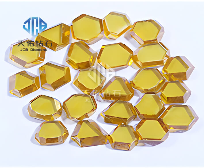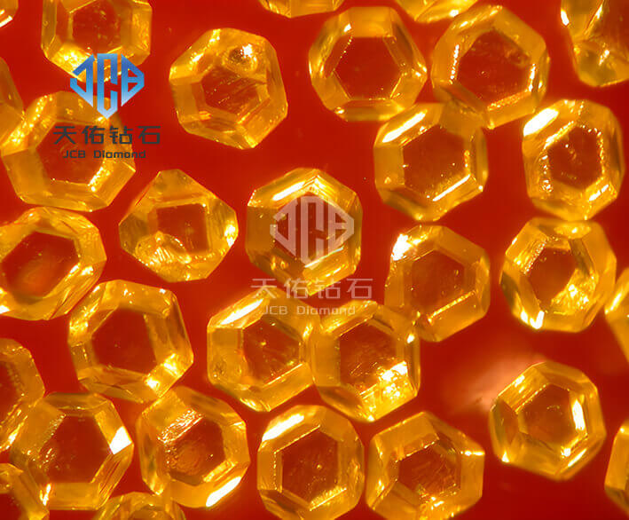


Product
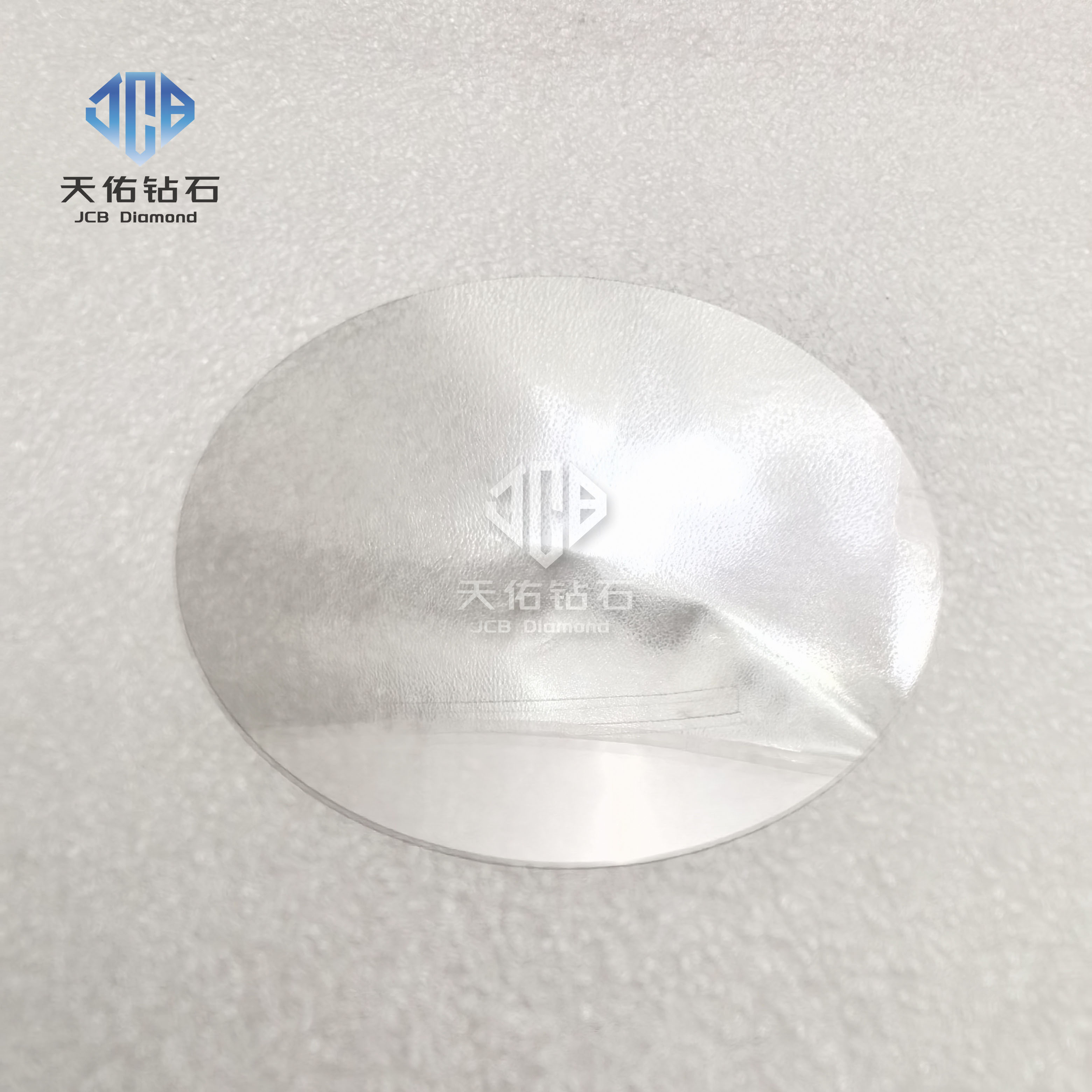
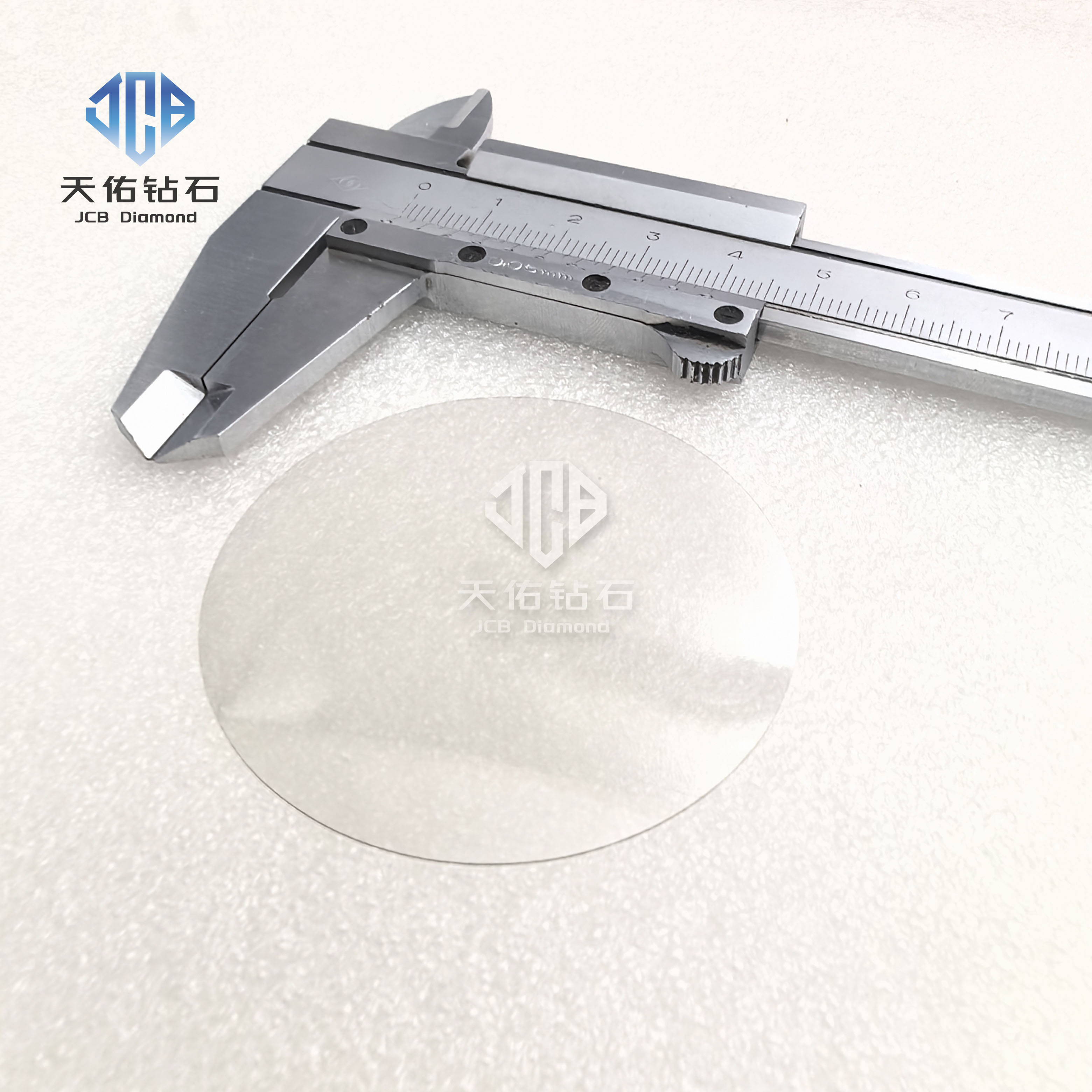
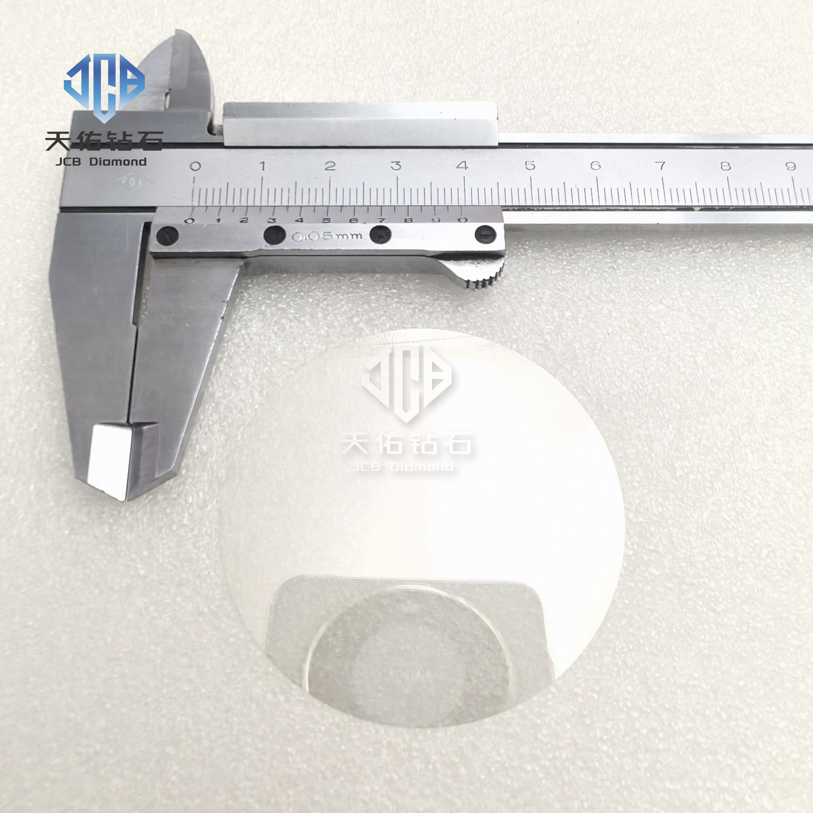
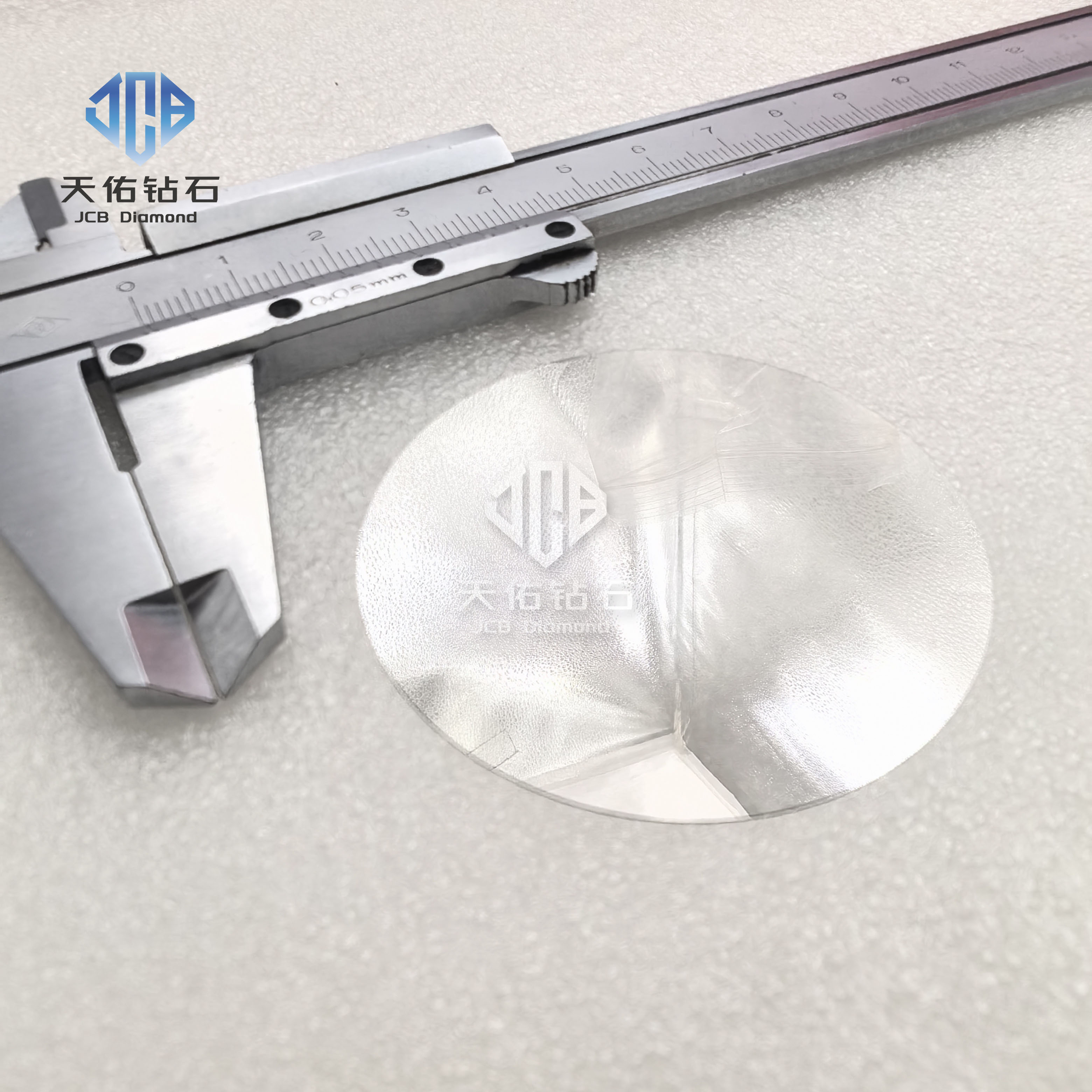
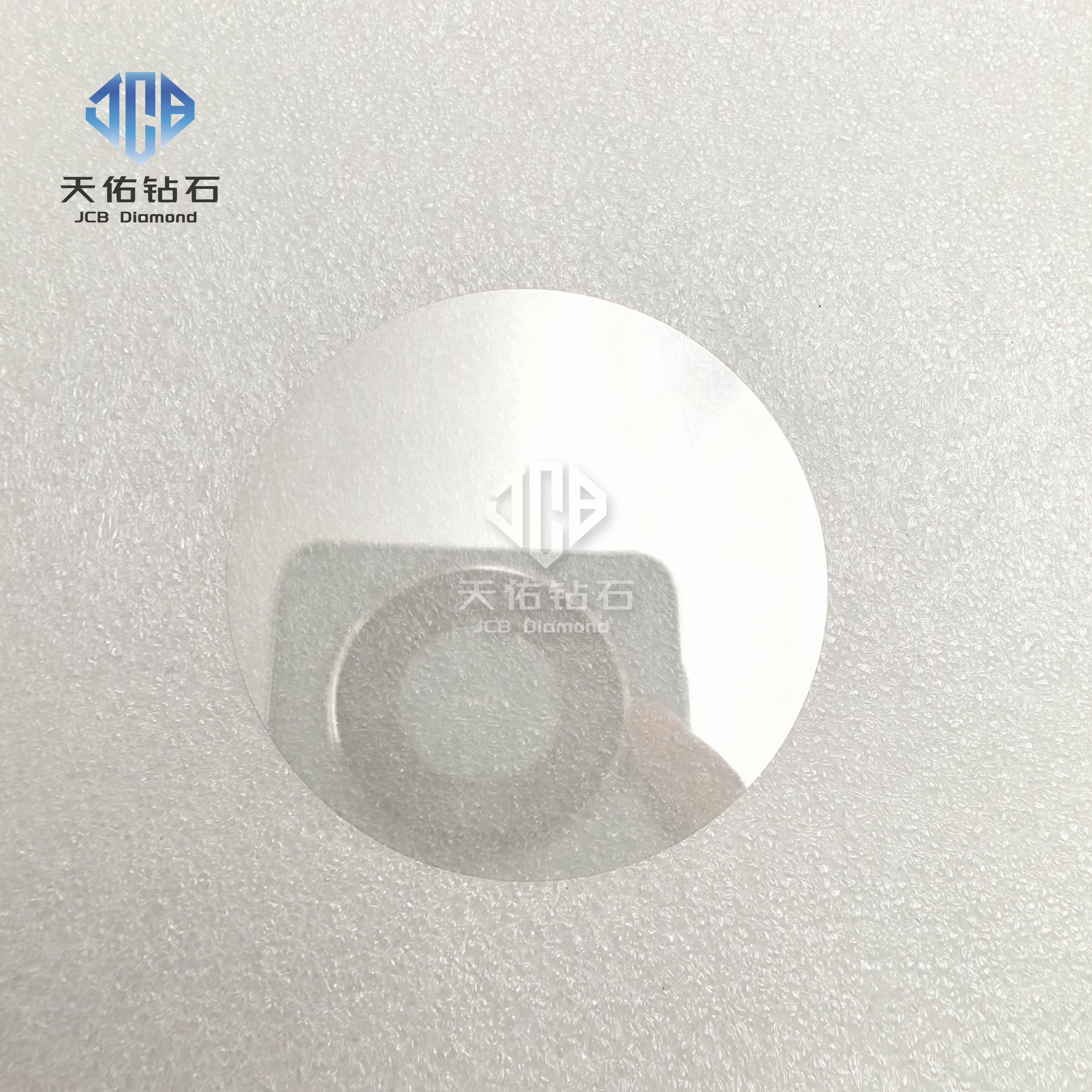
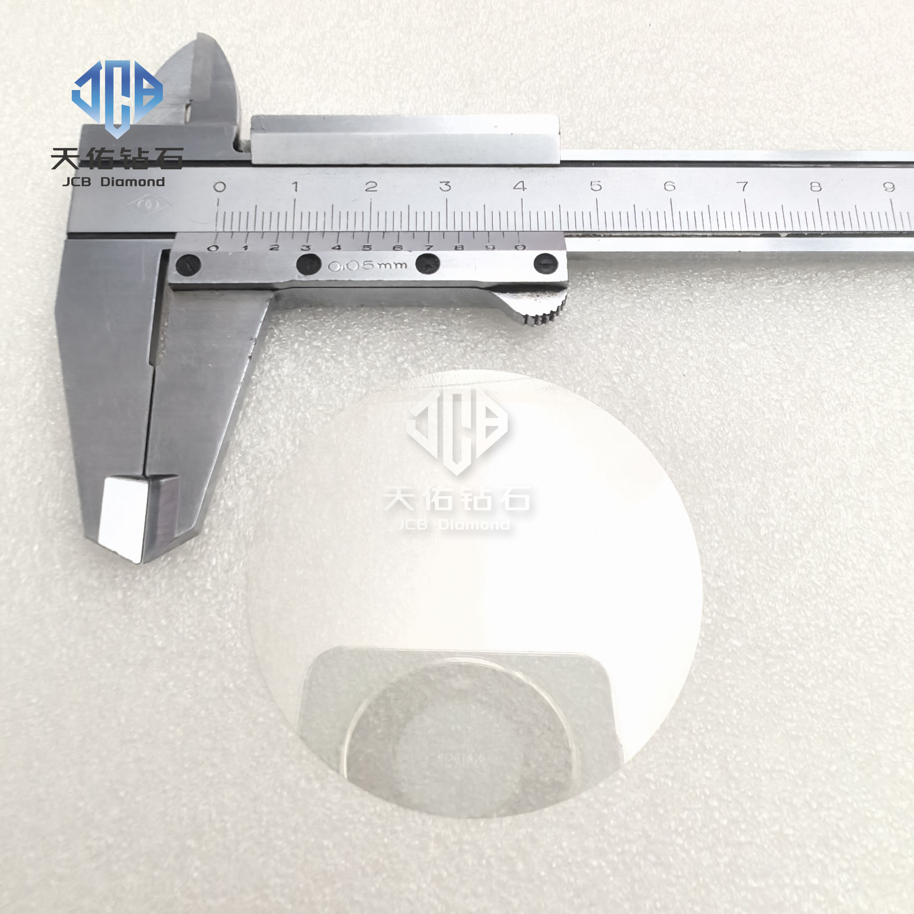
55*0.25mm
55*0.25mm
55*0.25mm
55*0.25mm
55*0.25mm
55*0.25mm
55*0.25mm
55*0.25mm
55*0.25mm
55*0.25mm
55*0.25mm

55*0.25mm

Diamond heat sinks combine exceptional thermal conductivity, electrical insulation, a low coefficient of thermal expansion, and resistance to high temperatures and corrosion, making them an ideal choice for cooling high-power electronic devices such as high-power semiconductor lasers, RF power amplifiers, AI computing chips, 5G/6G communication base stations, and power modules for new energy vehicles.

WeChat

Whatsapp

Product center

ParameterSpecification Range
Thermal Conductivity1000–2200 W/(m·K) @25°C (customizable grades: TC1200 / TC1500 / TC1800 / TC2000)
Coefficient of Thermal Expansion (CTE)0.8–1.0 ppm/K (well matched to Si, GaN)
Electrical Resistivity10¹⁴–10¹⁶ Ω·cm
Dielectric Constant~5.68 @1MHz
Dielectric Loss~6.2×10⁻⁸ @1MHz
Dielectric Strength≥11 kV/mm
Density3.52 g/cm³
Vickers Hardness>8000 kg/mm²
Young's Modulus850–1100 GPa
Tensile Strength450–1100 MPa
Thermal Diffusivity6.6–11.0 cm²/s (increases with thermal conductivity grade)
DimensionsCustomizable; supports 2 / 3 / 4 / 6‑inch wafers and non‑standard shapes; max size 120 mm × 120 mm
Thickness200–1000 μm (customizable)
Surface RoughnessGrowth side: Ra <1–30 nm (fine polishing down to <2 nm)
Nucleation side: Ra <30 nm
TTV (Total Thickness Variation)<60 μm (for 2‑inch; customizable)
Warpage<300 μm (for 2‑inch; customizable)


Specification:

ParameterSpecification Range
Thermal Conductivity1000–2200 W/(m·K) @25°C (customizable grades: TC1200 / TC1500 / TC1800 / TC2000)
Coefficient of Thermal Expansion (CTE)0.8–1.0 ppm/K (well matched to Si, GaN)
Electrical Resistivity10¹⁴–10¹⁶ Ω·cm
Dielectric Constant~5.68 @1MHz
Dielectric Loss~6.2×10⁻⁸ @1MHz
Dielectric Strength≥11 kV/mm
Density3.52 g/cm³
Vickers Hardness>8000 kg/mm²
Young's Modulus850–1100 GPa
Tensile Strength450–1100 MPa
Thermal Diffusivity6.6–11.0 cm²/s (increases with thermal conductivity grade)
DimensionsCustomizable; supports 2 / 3 / 4 / 6‑inch wafers and non‑standard shapes; max size 120 mm × 120 mm
Thickness200–1000 μm (customizable)
Surface RoughnessGrowth side: Ra <1–30 nm (fine polishing down to <2 nm)
Nucleation side: Ra <30 nm
TTV (Total Thickness Variation)<60 μm (for 2‑inch; customizable)
Warpage<300 μm (for 2‑inch; customizable)


Chat
If you have any questions, comments or feedback about the product, please fill out the form below, we will get back to you as soon as possible! Phone/wechat /Whatsapp:16697772369/16697772169
Email:
Name:
* Tel:
Country:
* Content:
Copyright © 2013 Henan JCB Superhard Material Co., Ltd 51统计入口

Home
Tel
Message